

Display device and electronic appliance
a technology of electronic appliances and display devices, applied in static indicating devices, instruments, organic semiconductor devices, etc., can solve problems such as affecting the reduction of power consumption, and achieve the effect of reducing the drive voltage of light emitting elements and reducing power consumption
- Summary
- Abstract
- Description
- Claims
- Application Information
AI Technical Summary
Benefits of technology
Problems solved by technology
Method used
Image

Examples
embodiment mode 1
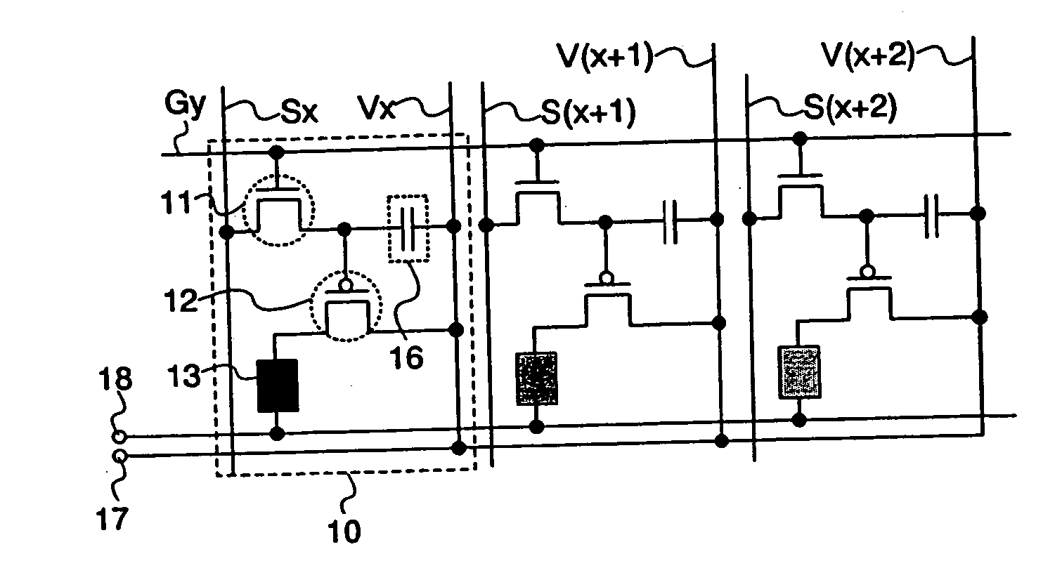
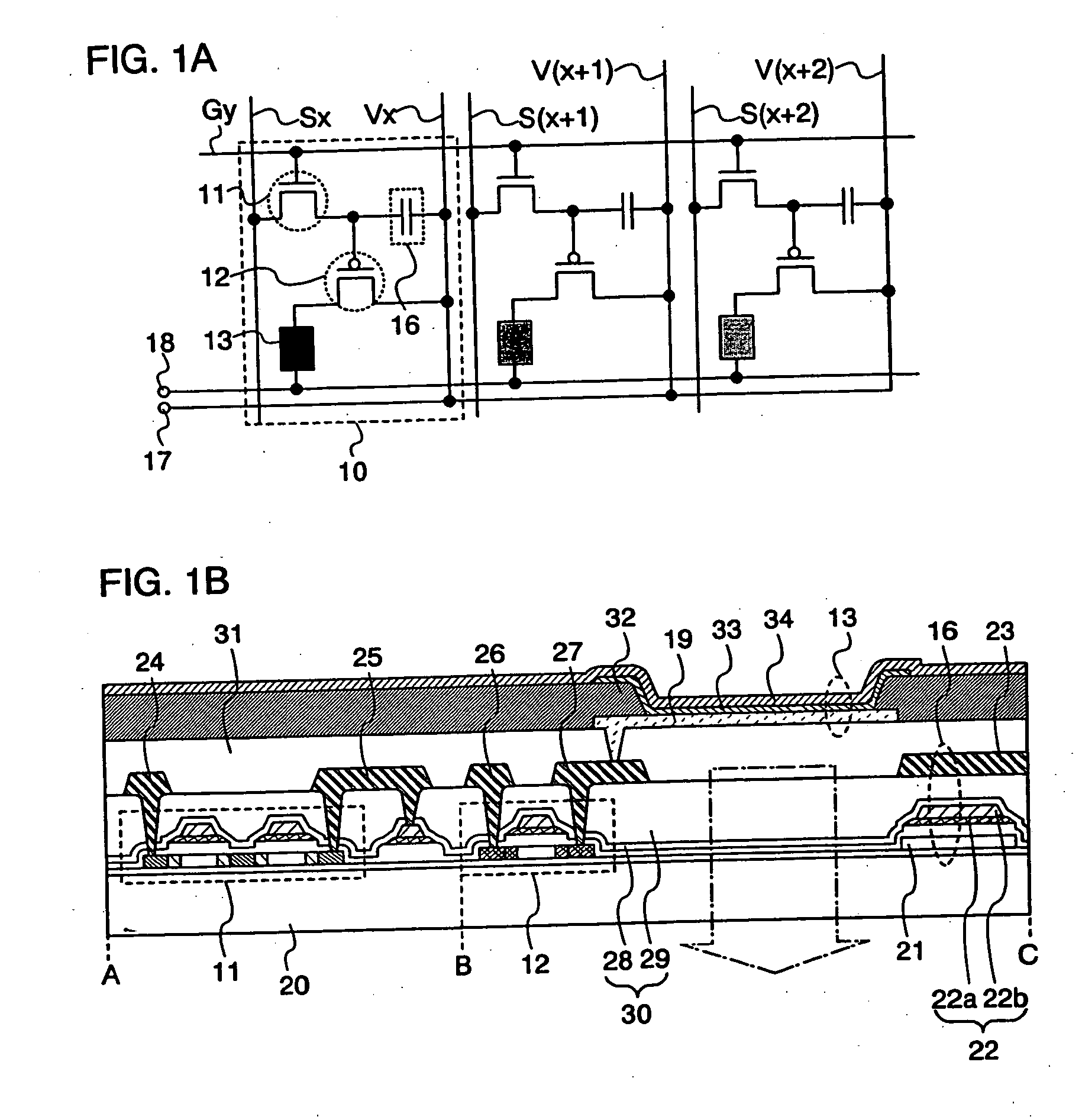
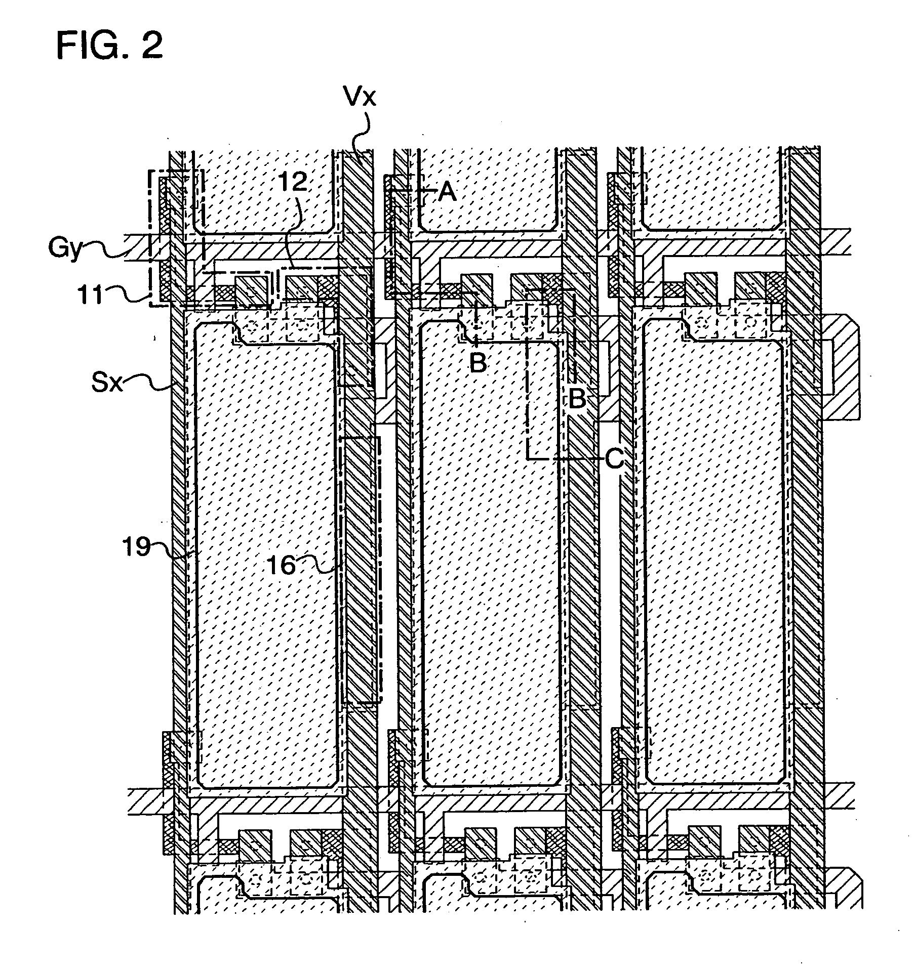
[0070] The structure of a display device in accordance with a preferred embodiment of the invention is described below with reference to FIGS. 1A to 3. The display device of the invention comprises a plurality of pixels 10 each including a plurality of elements in the region where a source line Sx (x is a natural number, and 1≦x≦m is satisfied) and a gate line Gy (y is a natural number, and 1≦y≦n is satisfied) cross each other with an insulator interposed therebetween (see FIG. 1A). The pixel 10 includes a light emitting element 13, a capacitor 16 and two transistors. One of the two transistors is a switching transistor 11 (hereinafter also referred to as a TFT 11) for controlling a video signal input to the pixel 10 and a driving transistor 12 (hereinafter also referred to as a TFT 12) for controlling emission / non-emission of the light emitting element 13. Each of the TFTs 11 and 12 is a field effect transistor that has three terminals of a gate electrode, a source electrode and a ...
embodiment mode 2
[0099] The aforementioned configuration employed the case where the TFT 12 is a P-channel TFT. In this embodiment mode, description is made with reference to FIGS. 19A to 19C on the case where the TFT 12 is an N-channel TFT. The pixel 10 includes the light emitting element 13, the capacitor 16 and the TFTs 11 and 12 (see FIG. 19A). When the light emitting element 13 has a forward stacking structure (when the pixel electrode is an anode while the counter electrode is a cathode), and a forward bias voltage is applied to the light emitting element 13 in accordance with the current flow direction of the light emitting element 13, the first power source 17 corresponds to a high potential power source while the second power source 18 corresponds to a low potential power source. When a reverse bias voltage is applied to the light emitting element 13, on the other hand, the first power source 17 is a low potential power source while the second power source 18 is a high potential power sourc...
embodiment mode 3
[0103] Description is made now with reference to FIGS. 5 to 7 on the configuration of the source driver 43 included in the display device of the invention. The source driver 43 includes the pulse output circuit 44, a NAND 71, the first latch 47, the second latch 48 and the selection circuit 46 (the first latch 47, the second latch 48 and the selection circuit 46 are collectively referred to as an SLAT in the drawing) (see FIG. 5). The pulse output circuit 44 has a configuration in which a plurality of unit circuits (SSR) 70 are connected in cascade. The pulse output circuit 44 is supplied with a clock signal (SCK), a clock back signal (SCKB) and a start pulse (SSP). The first latch 47 is supplied with data signals (DataR, DataG and DataB). The second latch 48 is supplied with a latch pulse (SLAT), and an inverted pulse of the latch pulse (SLATB). The selection circuit 46 is supplied with a writing / erasing signal (SWE or Write / Erase signal, hereinafter also referred to as a WE signal...
PUM
 Abstract
Description
Claims
Application Information