Light emitting device and manufacturing method thereof

a technology of light emitting device and manufacturing method, which is applied in the direction of discharge tube luminescnet screen, discharge tube/lamp details, electric discharge lamps, etc., can solve the problems of reliability, easy deterioration of light emitting elements, and affecting the use of light emitting devices, so as to reduce the amount of water remaining inside the light emitting device, and suppress the effect of light emitting element deterioration

Inactive Publication Date: 2005-09-29
SEMICON ENERGY LAB CO LTD
View PDF18 Cites 24 Cited by
  • Summary
  • Abstract
  • Description
  • Claims
  • Application Information

AI Technical Summary

Benefits of technology

[0007] It is an object of the present invention to provide a structure and a manufacturing method of a light emitting device, which reduces the amount of water remaining in the light emitting device.
[0008] It is another object of the invention to provide a structure and a manufacturing method of a light emitting device, which suppresses the deterioration of a light emitting element due to water remaining in the light emitting device.
[0024] In a light emitting device having a structure of the invention, the amount of water remaining inside the light emitting device is reduced. Further, the deterioration of a light emitting element due to water remaining inside can be suppressed.
[0025] In a light emitting device manufactured by a method for manufacturing a light emitting element of the present invention, the amount of water remaining inside the light emitting device is reduced. Further, the deterioration of a light emitting element due to water remaining inside can be suppressed.

Problems solved by technology

However, one background of not reaching practical use yet while having such big advantages is a problem of reliability.
The light emitting element often deteriorates due to moisture (water) and has a disadvantage of being hard to obtain long-term reliability.
It is conceivable that this causes a dark spot (black spot) and shrinkage (a decrease in luminance from an edge portion of a display device) in a display device using the light emitting element.
However, these countermeasures are insufficient and have few effects on a defect that a region where emission intensity is decreased is gradually increased with time.

Method used


Image

  • Light emitting device and manufacturing method thereof
  • Light emitting device and manufacturing method thereof
  • Light emitting device and manufacturing method thereof

Examples


embodiment mode 1

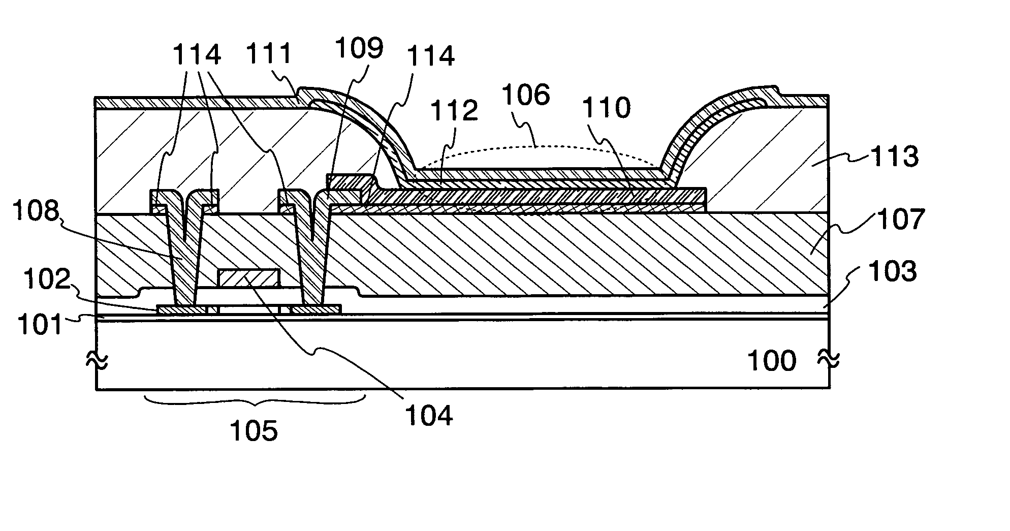
[0040]FIGS. 1A and 1B are cross-sectional views showing part of a light emitting device of the invention. A light emitting device of the invention includes: a base insulating layer 101 formed over a substrate 100; a thin film transistor 105 having a semiconductor layer 102 formed over the base insulating layer 101 as an active layer, a gate insulating layer 103, and a gate electrode 104; and a light emitting element 106. The thin film transistor 105 is covered with an insulating layer 107. Over the insulating layer 107, electrodes 108 and 109 of the thin film transistor 105 which electrically connect to the semiconductor layer 102 through contact holes penetrating the insulating layer 107 and the gate insulating layer 103, and a wiring (not shown) are formed. Note that the wiring may be formed at the same time as the electrodes 108 and 109, but may be separately formed. A first electrode 110 of the light emitting element 106 is formed to partially overlap and electrically connect to...

embodiment mode 2

[0064] A method for manufacturing a light emitting element of the invention is described in this embodiment mode with reference to FIGS. 3A to 3D and FIGS. 4A to 4D.

[0065] An insulating layer 801 is formed over a substrate 800, and a semiconductor layer is then formed over the insulating layer 801 (FIG. 3A).

[0066] Light transmitting glass, quartz, plastic (such as polyimide, acrylic, polyethylene terephthalate, polycarbonate, polyacrylate, or polyethersulfone), or the like can be used as a material of the substrate 800. The substrate thereof may be used after being polished by CMP or the like, if necessary. In this embodiment mode, a glass substrate is used.

[0067] The insulating layer 801 is formed in order to prevent an element exerting an adverse influence on characteristics of the semiconductor layer, such as an alkali metal or an alkaline earth metal contained in the substrate 800, from diffusing into the semiconductor layer. Silicon oxide, silicon nitride, silicon oxide cont...

embodiment mode 3

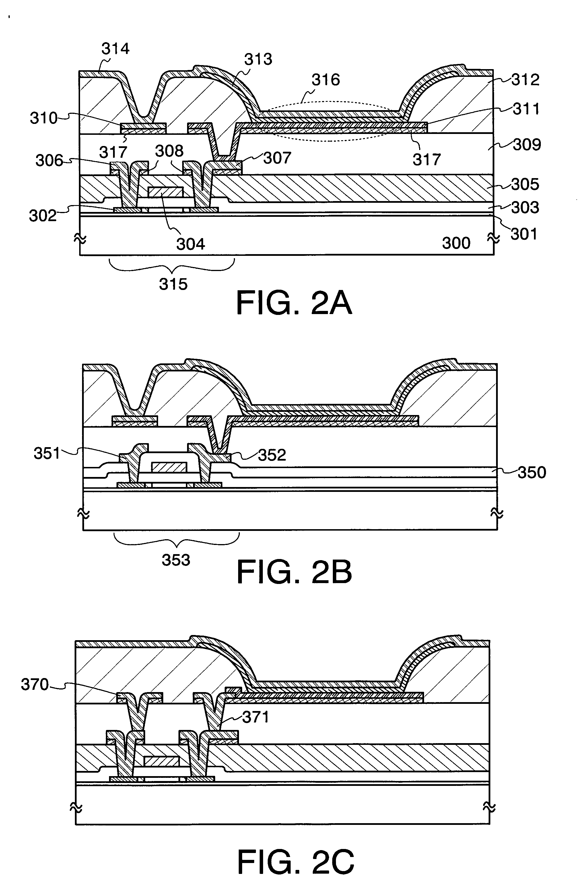
[0108] A method for manufacturing a light emitting device having the structure shown in FIG. 2B is described in this embodiment mode with reference to FIGS. 5A to 5D. Description up to formation of a base insulating layer 801, a semiconductor layer 802, a gate insulating layer 803, and a gate electrode 804 over a substrate 800 (FIG. 5A) is similar to the description of FIG. 3A in Embodiment Mode 2; therefore, the description is omitted here.

[0109] After forming the gate electrode 804, a first insulating layer 850 is formed. The first insulating layer 850 can be formed of an organic insulating layer of acrylic or polyimide, an inorganic insulating layer mainly containing silicon oxide or silicon nitride, siloxane, or the like. In this embodiment mode, silicon oxide is used for the first insulating layer 850. In the case of forming the first insulating layer 850 by applying a self-planarizing material of acrylic, polyimide, siloxane, or the like, the light emitting device has such a ...


PUM


Abstract

An object of the present invention is to provide a structure and a manufacturing method of a light emitting device, which reduces the amount of water remaining in the light emitting device. Another object of the invention is to provide a structure and a manufacturing method of a light emitting device, which suppresses the deterioration of a light emitting element due to water remaining in the light emitting device. A light emitting device of the invention includes a thin film transistor, an insulating layer covering the thin film transistor, an electrode which is electrically connected to the thin film transistor through a contact hole formed on the insulating layer, and a light emitting element formed by interposing a light emitting layer between a first electrode which is electrically connected to the electrode and a second electrode. The light emitting device further includes a layer formed of a different material from that of the insulating layer only between the electrode and the first electrode over the insulating layer and the insulating layer.

Description

BACKGROUND OF THE INVENTION [0001] 1. Field of the Invention [0002] The present invention relates to a display device which is manufactured by using an element having a light emitting material interposed between electrodes and emitting light by applying an electric current between the electrodes (light emitting element). [0003] 2. Description of the Related Art [0004] In recent years, a thin lightweight display using a light emitting element has been actively developed. The light emitting element is manufactured by interposing a material which emits light by applying an electric current between a pair of electrodes. Since the light emitting element itself emits light unlike in the case of liquid crystal, a light source such as back light is not required, and the element is very thin. Therefore, it is extremely advantageous to manufacture a thin lightweight display. [0005] However, one background of not reaching practical use yet while having such big advantages is a problem of relia...

Claims


Application Information

Patent Timeline
Patent Type & Authority Applications(United States)
IPC IPC(8): H01J63/04H01L21/77H01L27/32H01L51/52H05B33/04H05B33/10H05B33/12
CPCH01L27/3248H01L27/3258H05B33/04H01L51/5253H01L27/1248H01L27/3244H01L27/1214H10K59/123H10K59/124H10K50/844H10K59/12
Inventor SAKAKURA, MASAYUKITAKAHASHI, SHUHEIIKEDA, KAZUKOFUTAMURA, TOMOYA
Owner SEMICON ENERGY LAB CO LTD
Why Eureka
Try Eureka