Semiconductor device

a technology of semiconductor devices and dielectric capacitors, applied in the direction of dismountable cabinets, process and machine control, instruments, etc., can solve the problems of reducing the size of dc-dc converters, affecting the performance of dc-dc converters, and affecting the proportion of losses, so as to reduce the number of parts, influence the high frequency characteristics, and reduce the effect of siz

Active Publication Date: 2005-10-06
RENESAS ELECTRONICS CORP
View PDF12 Cites 75 Cited by
  • Summary
  • Abstract
  • Description
  • Claims
  • Application Information

AI Technical Summary

Benefits of technology

[0033] Advantageous effects obtained by a representative one of the inventions disclosed in the present application will hereinafter be described in brief as follows:
[0034] In the present invention, a power transistor (first field effect transistor) for a high side switch, a power transistor (second field effect transistor) for a low side switch, and driver circuits (control circuits) that drive these are respectively constituted of different first through third semiconductor chips. Further, the three semiconductor chips are accommodated or held in one package. Furthermore, the first semiconductor chip including th...

Problems solved by technology

Thus, there is a fear that a size reduction of the DC-DC converter cannot be achieved sufficiently.
Further, there is a fear that since there is a need to route wirings on a mounting board to connect the two different packages, losses occur due to inductances parasitized on the routing wirings and hence the efficiency of voltage conversion will be degraded.
The proportion of the losses is particularly noticeable where an increase in high fre...

Method used


Image

  • Semiconductor device
  • Semiconductor device
  • Semiconductor device

Examples


first preferred embodiment

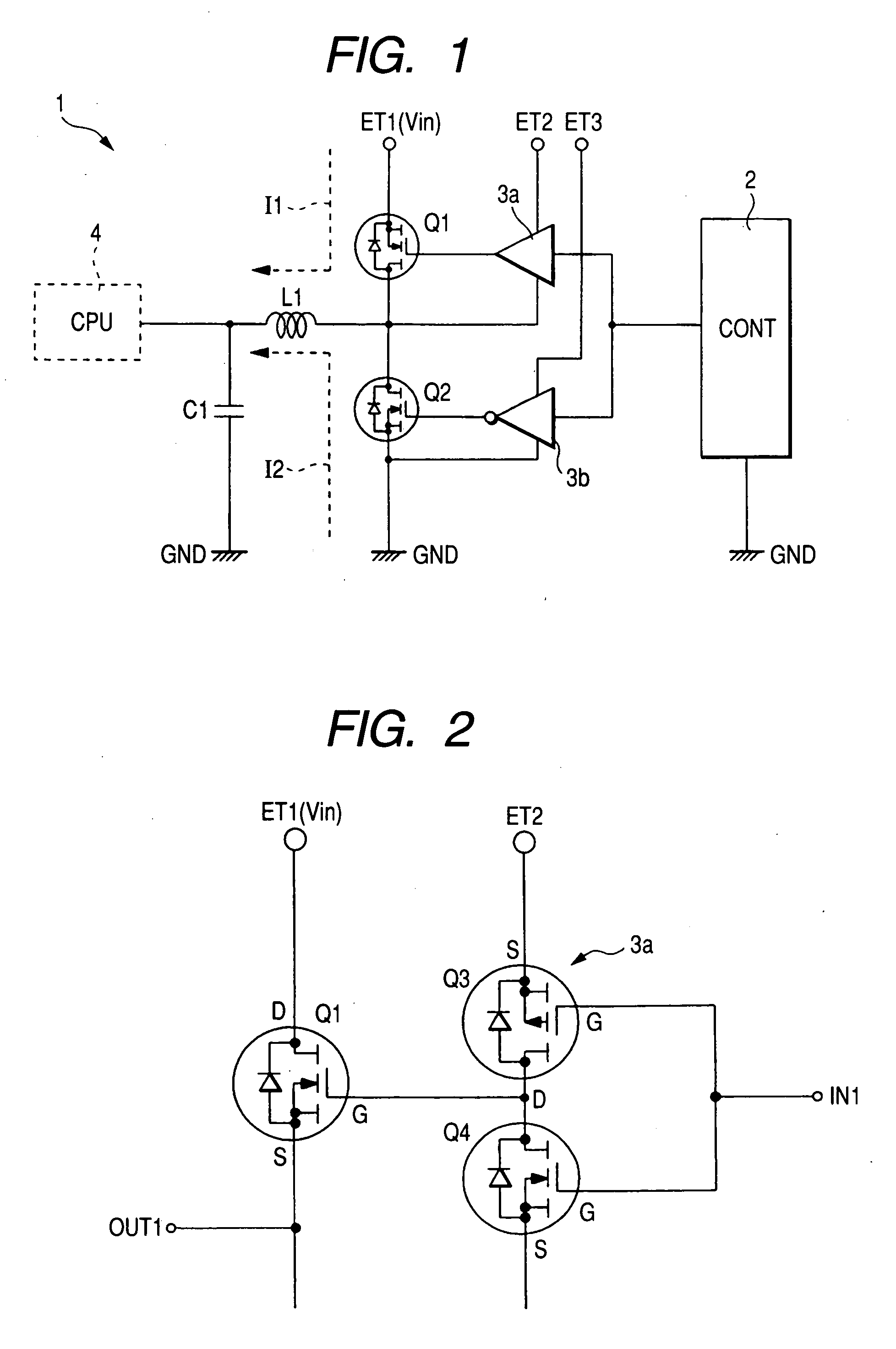
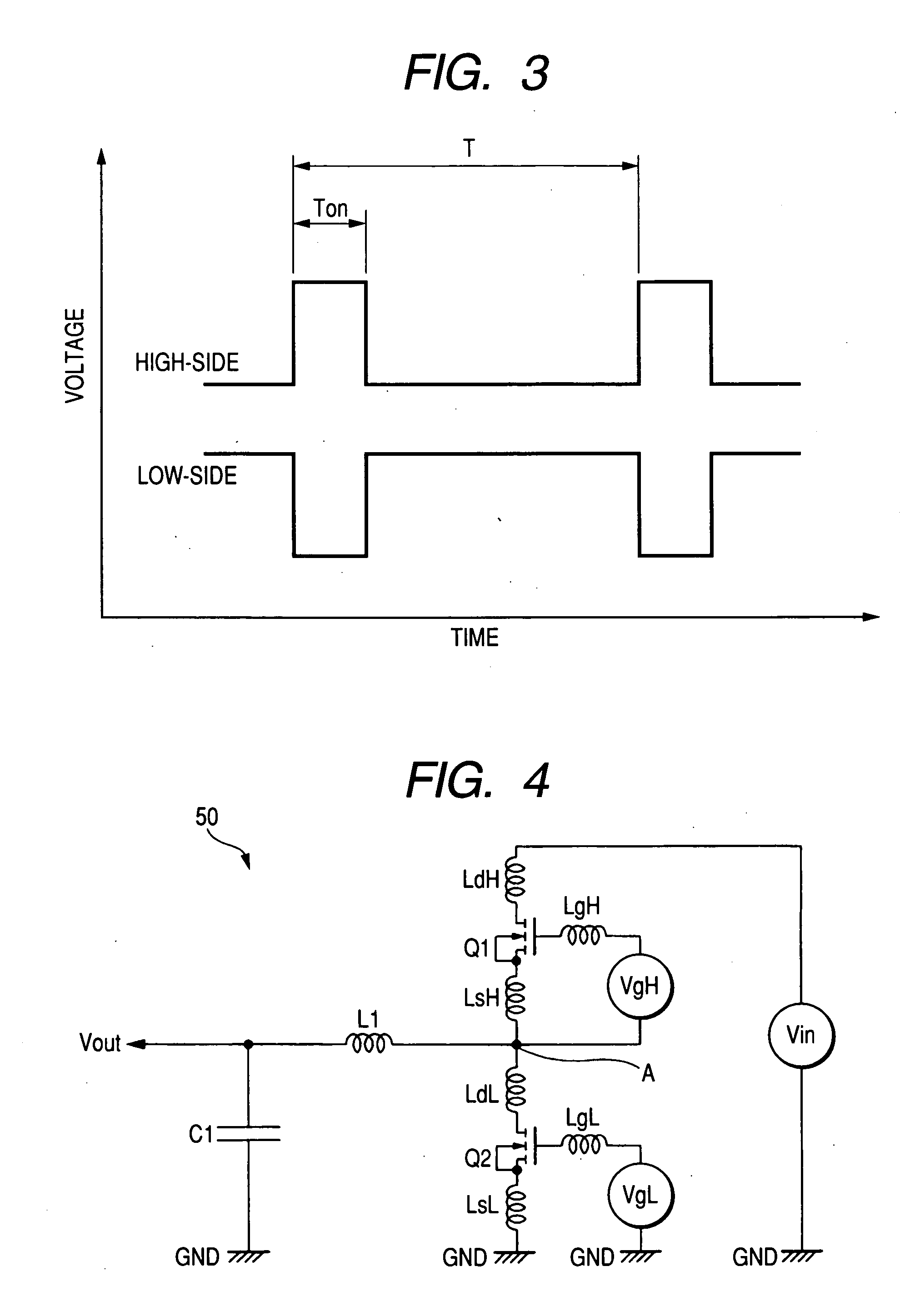
[0090] A semiconductor device according to a first embodiment is of, for example, a non-insulated type DC-DC converter employed in a power supply circuit for a disk top type personal computer, a notebook-size personal computer, a server or a game machine or the like. FIG. 1 shows a circuit diagram of one example of the non-insulated type DC-DC converter. The non-insulated type DC-DC converter has elements like a control circuit 2, driver circuits 3a and 3b, field effect transistors (power MOS•FETs) Q1 and Q2, a coil L1, a condenser or capacitor C1, etc. These elements are mounted on a wiring board and electrically connected to one another through wirings of the wiring board. Incidentally, reference numeral 4 in FIG. 1 indicates a load circuit like a CPU (Central Processing Unit) or DSP (Digital Signal Processor) for the disk top type personal computer, notebook-size personal computer, server or game machine. Symbols ET1, ET2 and ET3 indicate terminals respectively. As shown in FIG. ...

second preferred embodiment

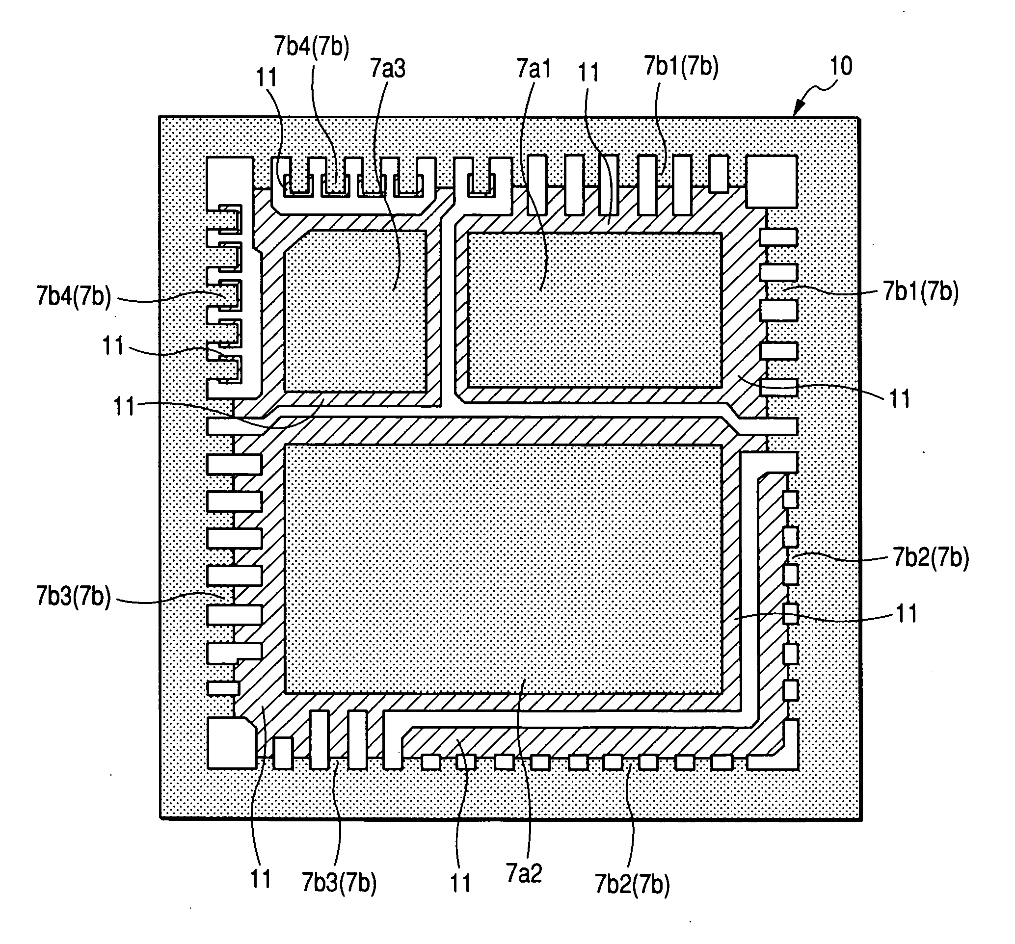
[0160]FIG. 28 is a plan view showing one example of a package configuration of a semiconductor device according to a second embodiment of the present invention. The semiconductor device described in FIG. 28 is substantially similar to the semiconductor device shown in FIG. 8 in configuration but principally different therefrom in terms of the shape of a gate electrode pad BP3 in a semiconductor chip 5a, the shapes of a gate electrode pad BP7 and a source electrode pad BP5b in a semiconductor chip 5b, portions covered with surface protection films 14 and 22 in the semiconductor chips 5a and 5b, the shape of a source cell area, etc. Incidentally, FIG. 28 is also shown excepting the semiconductor chips 5a, 5b and 5c, die pads 7a1, 7a2 and 7a3 and resin encapsulation body 8 placed over leads 7b in order to make it easy to see the drawing. Further, the die pads 7a1, 7a2 and 7a3 and leads 7b are given hatching.

[0161] In the second embodiment, a source electrode pad BP5 (BP5a) connected t...

third preferred embodiment

[0166]FIG. 29 is a plan view showing one example of a package configuration of a semiconductor device according to a third embodiment of the present invention. The semiconductor device described in FIG. 29 is substantially similar to the semiconductor device shown in FIG. 8 in configuration but principally different therefrom in terms of a gate electrode pattern in a semiconductor chip 5a. Incidentally, FIG. 29 is also shown excepting the semiconductor chips 5a, 5b and 5c, die pads 7a1, 7a2 and 7a3 and resin encapsulation body 8 placed over leads 7b in order to make it easy to see the drawing. Further, the die pads 7a1, 7a2 and 7a3 and leads 7b are given hatching.

[0167] In the third embodiment, the width of a portion (first wiring and first portion) BP3a formed between two source electrode pads BP1 in the gate electrode pattern electrically connected to a gate electrode pad BP3 of a first field effect transistor Q1 for a high side switch is formed thicker than the width of a portio...


PUM


Abstract

The present invention provides a non-insulated type DC-DC converter having a circuit in which a power MOS•FET for a high side switch and a power MOS•FET for a low side switch are connected in series. In the non-insulated type DC-DC converter, the power transistor for the high side switch, the power transistor for the low side switch, and driver circuits that drive these are respectively constituted by different semiconductor chips. The three semiconductor chips are accommodated in one package, and the semiconductor chip including the power transistor for the high side switch, and the semiconductor chip including the driver circuits are disposed so as to approach each other.

Description

CROSS-REFERENCE TO RELATED APPLICATION [0001] The present invention claims priority from Japanese patent application No. 2004-106224 filed on Mar. 31, 2004, the content of which is hereby incorporated by reference into this application. BACKGROUND OF THE INVENTION [0002] The present invention relates to a semiconductor device technique, and particularly to a technique effective when applied to a semiconductor device having a power supply circuit. [0003] In order to attain adaptation to miniaturization of a power supply circuit or the like and its fast response, a power MOS•FET (Metal Oxide Semiconductor Field Effect Transistor) used in a power supply has been proceeding toward an increase in high frequency in recent years. [0004] In particular, a non-insulated type DC-DC converter used as a power supply circuit for a desk top type or notebook personal computer, a-server or a game machine or the like has a tendency to increase in current and frequency with respect to a CPU (Central P...

Claims


Application Information

Patent Timeline
IPC IPC(8): H01L25/07H01L21/8234H01L23/02H01L23/495H01L23/50H01L25/00H01L25/16H01L25/18H01L27/04H01L27/088H01L29/78H02M3/155H02M3/158
CPCH01L23/49575H01L2924/1306H01L24/45H01L24/49H01L25/165H01L2224/29339H01L2224/45015H01L2224/45144H01L2224/48091H01L2224/48095H01L2224/48137H01L2224/48247H01L2224/4903H01L2224/49051H01L2224/49111H01L2224/49171H01L2224/49175H01L2224/4943H01L2224/83855H01L2924/01002H01L2924/01004H01L2924/01005H01L2924/01006H01L2924/01013H01L2924/01014H01L2924/01015H01L2924/0102H01L2924/01028H01L2924/01029H01L2924/01033H01L2924/01046H01L2924/01047H01L2924/0105H01L2924/01078H01L2924/01079H01L2924/01082H01L2924/13091H01L2924/14H01L2924/19041H01L2924/19042H01L2924/19043H01L2924/20753H01L2924/20755H01L2924/30105H01L2924/30107H01L2924/3011H02M3/1588Y02B70/1466H01L24/48H01L2924/01023H01L2924/014H01L2224/85H01L2224/45147H01L29/4175H01L24/85H05K7/02H01L2224/05554H01L23/5386H01L23/50H01L2924/00014H01L2924/00H01L2924/00012H01L2924/181H01L2224/85203H01L2224/85205H01L2224/0603Y02B70/10H01L2224/40245H01L2924/18301H01L2924/2075H01L2924/20754A47F5/101A47B47/00A47B96/028A47B96/061
Inventor SATOU, YUKIHIROUNO, TOMOAKIMATSUURA, NOBUYOSHISHIRAISHI, MASAKI
Owner RENESAS ELECTRONICS CORP
Why Eureka
Try Eureka