Semiconductor device and method of fabricating the same

a semiconductor device and semiconductor technology, applied in the field of semiconductor devices, can solve the problems of current collapse, surface level structural defect, instability of the semiconductor device, etc., and achieve the effects of enhanced chemical vapor deposition, and high characteristic requirements

Active Publication Date: 2005-10-06
SUMITOMO ELECTRIC DEVICE INNOVATIONS
View PDF12 Cites 44 Cited by
  • Summary
  • Abstract
  • Description
  • Claims
  • Application Information

AI Technical Summary

Benefits of technology

[0013] The present invention has been made in view of the above-mentioned circumstances and it is a general object of the present invention to provide a SiN protection film effective for surface stabilization of a nitride semiconductor device, in particular, a nitride semiconductor device of GaN-type, which includes GaN or a mixed crystal including GaN such as AlGaN, InGaN, or InAlGaN.
[0014] A more specific object of the present invention is to provide a semiconductor device and a fabricating method thereof so that a gate leakage current and a current collapse are suppressed to a commercial level that satisfies high characteristic requirements.
[0015] According to an aspect of the present invention, preferably, there is provided a semiconductor device comprising a silicon nitride (SiN) film provided on a crystal surface of a nitride semiconductor. The SiN film has a hydrogen content equal to ...

Problems solved by technology

However, the nitride semiconductor device has some unsolved problems of instability deeply related to the surface such as current collapse and gate leakage.
This causes the surface level having a structural defect.
However, the current collapse can be suppressed significantly by the surface passivation with a SiN film, and so it is often considered that the current collapse results from the change in a charging state at the surface defect level.
Both of the gate leakage current and the current collapse...

Method used


Image

  • Semiconductor device and method of fabricating the same
  • Semiconductor device and method of fabricating the same
  • Semiconductor device and method of fabricating the same

Examples


Embodiment Construction

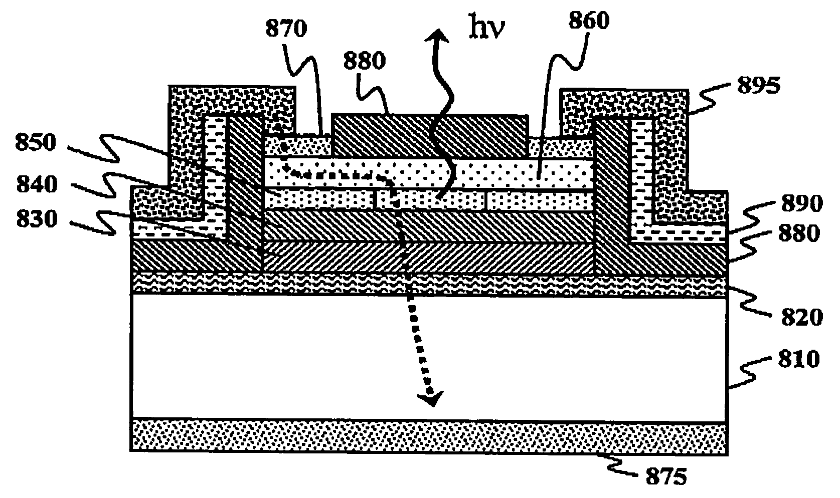
[0027] A description will now be given, with reference to the accompanying drawings, of embodiments of the present invention. In the following description, a silicon nitride film SiNx will be simply described as SiN, however, SiN does not denote only the specific case where the composition ratio of silicon and nitrogen in the silicon nitride film is 1:1.

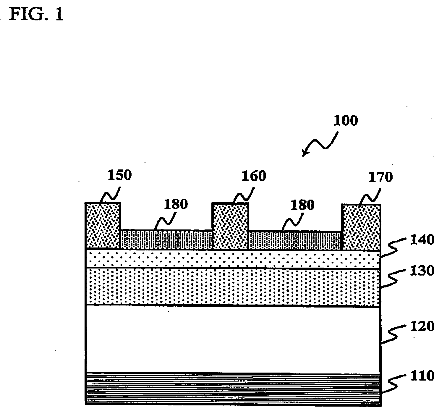
[0028]FIG. 1 illustrates a structural example of the nitride semiconductor device in accordance with the present invention. A nitride semiconductor device 100 includes an epitaxially grown electron traveling layer 120, an n-type AlGaN electron supply layer 130, and an n-type GaN thin film layer 140. The epitaxially grown electron traveling layer 120, the n-type AlGaN electron supply layer 130, and the n-type GaN thin film layer 140 form a laminate structure, and are sequentially laminated on a main surface of a silicon carbide substrate 110. A source 150, a gate 160, and a drain 170 to be biased are provided and spaced apart from ea...


PUM


Abstract

A semiconductor device includes a silicon nitride (SiN) film provided on a crystal surface of a nitride semiconductor, the SiN film having a hydrogen content equal to or smaller than 15 percent.

Description

BACKGROUND OF THE INVENTION [0001] 1. Field of the Invention [0002] This invention generally relates to semiconductor devices and methods of fabricating the same, and more particularly, to a nitride semiconductor device having a silicon nitride film on a surface thereof as a protection film and a method of fabricating the same. [0003] 2. Description of the Related Art [0004] A miniaturized semiconductor device is demanding a higher voltage and a higher power density. A wide band gap semiconductor is highly expected and a number of studies have been made. The wide band gap semiconductor is, for example, silicon carbide (SiC) and a nitride semiconductor such as gallium nitride (GaN) or the like. [0005] In particular, the nitride semiconductor has been developed as an optical device and has been reduced to spectacular practice as a blue light-emitting diode. The nitride semiconductor represented by gallium nitride has characteristics of wide band gap and direct transition. Additionally...

Claims


Application Information

Patent Timeline
IPC IPC(8): H01L21/318H01L21/338H01L21/8242H01L29/20H01L29/51H01L29/778H01L29/812H01L33/06H01L33/32H01L33/44
CPCH01L29/2003H01L29/51H01L29/7787
Inventor TANAKA, MASAHIROKOMATANI, TSUTOMU
Owner SUMITOMO ELECTRIC DEVICE INNOVATIONS
Why Eureka
Try Eureka