Semiconductor light emitting device and method of manufacturing the same

Inactive Publication Date: 2005-10-13
STANLEY ELECTRIC CO LTD
View PDF19 Cites 25 Cited by
  • Summary
  • Abstract
  • Description
  • Claims
  • Application Information

AI Technical Summary

Benefits of technology

[0029] As described above, the semiconductor light emitting device can display minimal color irregularity and brightness fluctuation, and can actively suppress the radiation of light that is potentially harmful to humans. These attributes can be achieved, for example, by sealing the semiconductor light emitting device with a

Problems solved by technology

If even a small gap exists, then the resin can leak out of the cup through that gap, resulting in a defective product.
Particularly, when a plurality of cups are formed within a large casing to enable large volume batch production, ensuring the high level of surface precision necessary to ensure a tight contact between the top surface of the cups and the lid is extremely difficult.
Furthermore, the heat of the resin heat curing process can cause deformations such as expansion or warping of the casing and/or the lid, thereby destroying the contact between the two members, and deterioration in the production yield is thus unavoidable.
Even if prevention of such problems were possible, the associated costs would be considerable.
In addition, in order to increase the quantity of light emitted, the size of the light emitting element can be increased, and a larger current can be passed through the element, but there are practical limits to the size of the package.
This means the size of the cup in which the light emitting element is located is also limited, which causes an increase in the proportion of the internal capacity of the cup occupied by the light emitting element, when compared with conventionally size

Method used


Image

  • Semiconductor light emitting device and method of manufacturing the same
  • Semiconductor light emitting device and method of manufacturing the same
  • Semiconductor light emitting device and method of manufacturing the same

Examples


Example

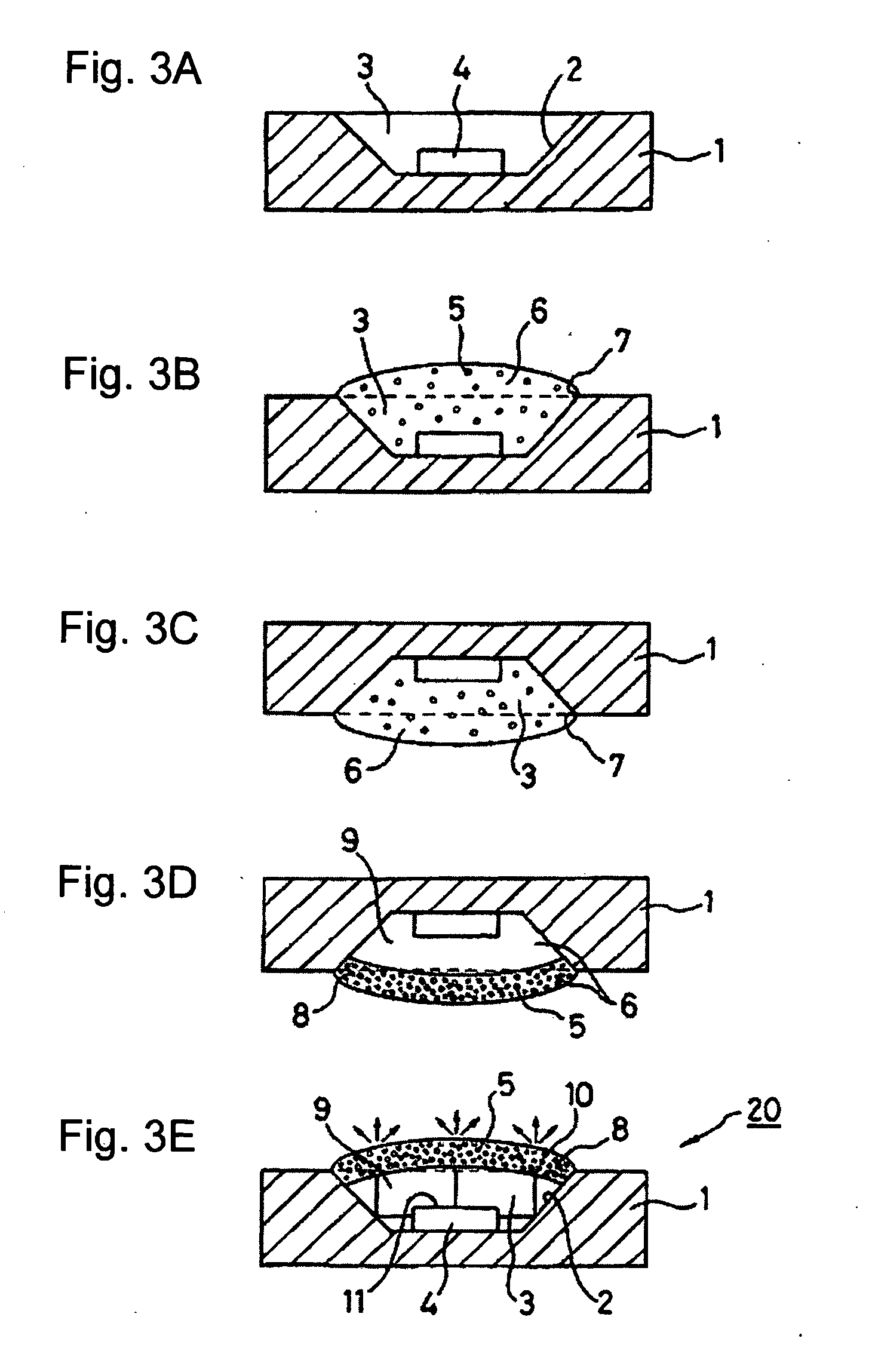
[0036] The following is a detailed description of exemplary embodiments of the invention, with reference to FIG. 3A through FIG. 3E, FIG. 4, and FIG. 5A through FIG. 5E. In these figures, identical members are labeled using the same symbols, and in some cases, descriptions of these common members are omitted. Although the following embodiments are exemplary of the invention, the invention is in no way limited to the embodiments presented below.

Exemplary Embodiment of FIGS. 3A-3E

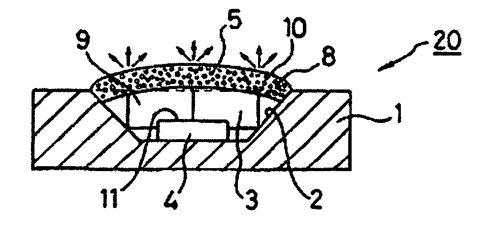
[0037]FIG. 3A through FIG. 3E are process diagrams showing an exemplary embodiment of a method of manufacturing a semiconductor light emitting device made in accordance with the principles of the invention. First, as shown in FIG. 3A, a cavity 3 can be formed in a casing 1 produced from an opaque resin with a high reflectance, and the inner peripheral surface of this cavity 3 can function as a reflective surface 2. A semiconductor light emitting element 4 can be disposed within the flat bottom portion of th...


PUM


Abstract

A semiconductor light emitting device can include a casing having a concave-shaped cavity with an opening, a semiconductor light emitting element installed in a bottom portion of the cavity, and a resin layer for filling an interior of the cavity. The resin layer can include a wavelength conversion material, and can be formed in a convex shape in a light radiation direction of the light emitting element. In the resin layer a layer with a high density of the wavelength conversion material can be formed near a surface of the convex shape

Description

[0001] This application claims the priority benefit under 35 U.S.C. § 119 of Japanese Patent Application No. 2004-106643 filed on Mar. 31, 2004, which is hereby incorporated by reference.BACKGROUND OF THE INVENTION [0002] 1. Field of the Invention [0003] The invention relates to a semiconductor light emitting device and a method of manufacturing such a device. More specifically, it relates to a semiconductor light emitting device that emits light of an arbitrary color, by using additive color mixing to combine the light emitted from a semiconductor light emitting element with the wavelength converted light emitted from a phosphor that has been excited by the light from the semiconductor light emitting element, as well as a method of manufacturing such a device. [0004] 2. Description of the Related Art [0005] Producing a white light emitting device using a light emitting diode (LED) chip that emits light with a sharp spectral distribution as the light source can be achieved by employ...

Claims


Application Information

Patent Timeline
IPC IPC(8): H01L33/60H01L33/54H01L33/50H01L27/15H01L33/32
CPCH01L33/508H01L2924/181H01L2924/00012
Inventor HARADA, MITSUNORI
Owner STANLEY ELECTRIC CO LTD
Why Eureka
Try Eureka