Semiconductor device with heterojunction

a technology of semiconductor devices and heterojunctions, which is applied in the direction of semiconductor devices, basic electric elements, electrical appliances, etc., can solve the problems of increasing the manufacturing cost of semiconductor devices, and achieve the characteristics of heterojunctions, increase the manufacturing cost of semiconductor devices, and close the crystallinity of hetero-semiconductor regions

Inactive Publication Date: 2005-10-13
NISSAN MOTOR CO LTD
View PDF0 Cites 45 Cited by
  • Summary
  • Abstract
  • Description
  • Claims
  • Application Information

AI Technical Summary

Benefits of technology

[0006] The closer the crystallinity of the hetero-semiconductor region to a single crystal the more the characteristics of the heterojunction provided by the related art improves. Namely, the reverse and forward characteristics of the related art are dependent on the impurity concentration and conductivity type of the hetero-semiconductor region. Forming a silicon single crystal or a silicon polycrystal composed of large grains on an SiC semiconductor substrate needs special expensive equipment such as a laser annealing apparatus or an MBE (molecular beam epitaxy) apparatus to increase the manufacturing cost of the semiconductor device. If the hetero-semiconductor region is formed without such special equipment or special processes, only a silicon polycrystal composed of fine grains will be formed on a {0001} crystal face of the substrate. A heterojunction formed with such silicon polycrystal will have limited characteristics. An object of the present invention is to solve this problem and provide a semiconductor device including a hetero-semiconductor region manufacturable at low cost and having large grains.

Problems solved by technology

Forming a silicon single crystal or a silicon polycrystal composed of large grains on an SiC semiconductor substrate needs special expensive equipment such as a laser annealing apparatus or an MBE (molecular beam epitaxy) apparatus to increase the manufacturing cost of the semiconductor device.

Method used


Image

  • Semiconductor device with heterojunction
  • Semiconductor device with heterojunction
  • Semiconductor device with heterojunction

Examples


first embodiment

[0027] First Embodiment

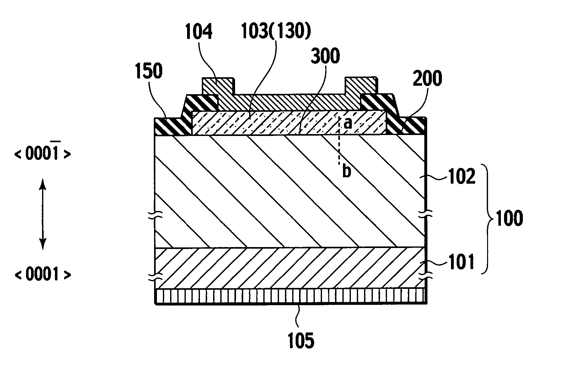
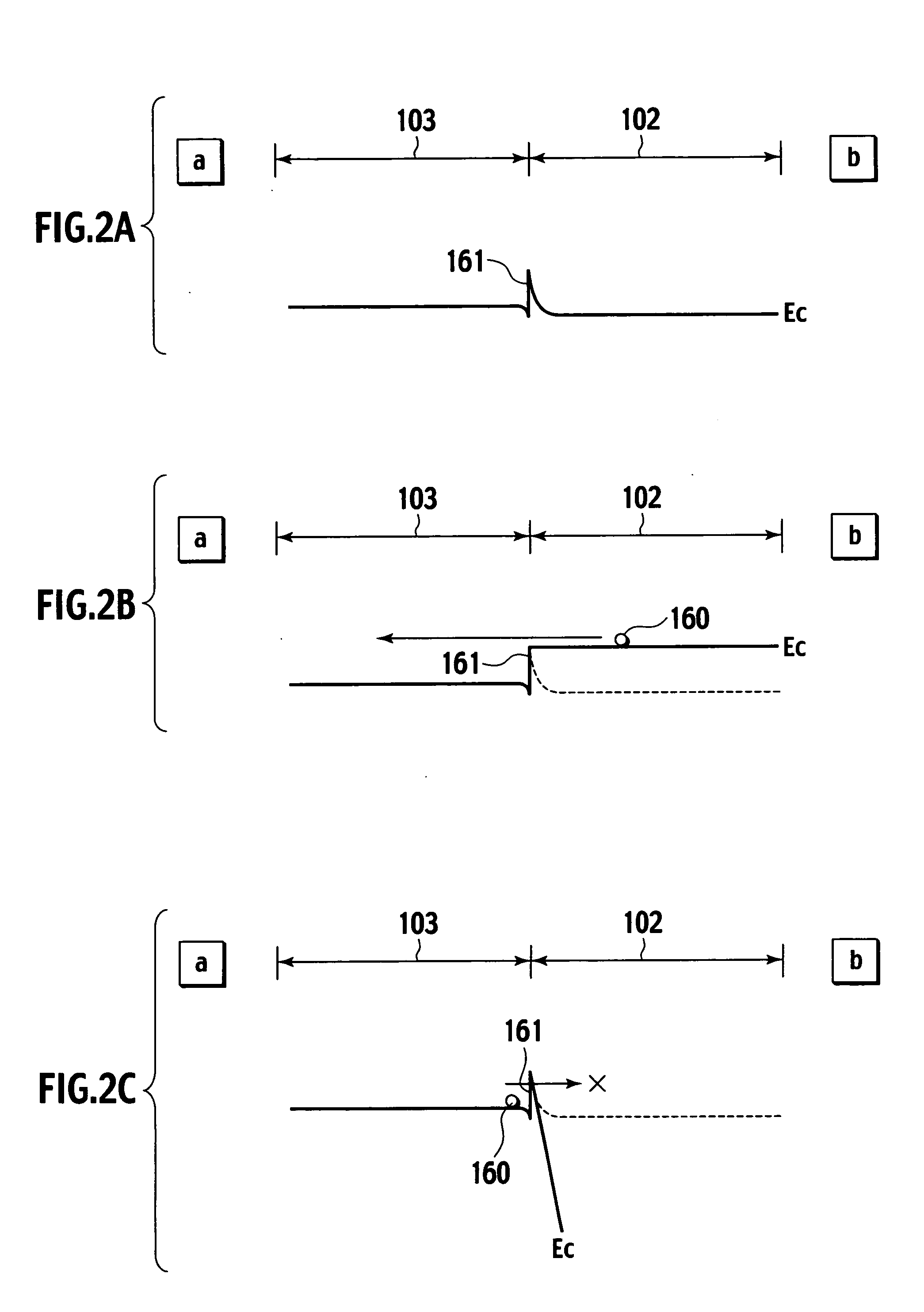
[0028]FIG. 1 is a sectional view showing a semiconductor device according to a first embodiment of the present invention. An n-type (first conductivity type) SiC substrate 101 and an n-type SiC epitaxial layer 102 whose impurity concentration is lower than that of the substrate 101 form an SiC semiconductor base 100. The SiC substrate 101 has, for example, a specific resistance of several to several hundreds of mΩ·cm and a thickness of several tens to several hundreds of μm. The SiC epitaxial layer 102 has, for example, an impurity concentration of 1×10¹⁵ to 1×1019 cm−3 and a thickness of several to several tens of μm. On the SiC epitaxial layer 102, a hetero-semiconductor region 103 is formed from an n-type silicon polycrystal film 130. The silicon polycrystal of the film 130 is a second semiconductor material that forms a heterojunction 300 with SiC of the epitaxial layer 102 and has a different band gap from SiC. The heterojunction 300 is formed on a {0001-...

second embodiment

[0044] Second Embodiment

[0045]FIG. 8 is a sectional view showing a semiconductor device according to a second embodiment of the present invention. An n-type (first conductivity type) SiC substrate 101 and an n-type SiC epitaxial layer 102 whose impurity concentration is lower than that of the substrate 101 form an SiC semiconductor base 100. The SiC substrate 101 has, for example, a specific resistance of several to several hundreds of mΩ·cm and a thickness of several tens to several hundreds of μm. The SiC epitaxial layer 102 has, for example, an impurity concentration of 1×10¹⁵ to 1×1019 cm−3 and a thickness of several to several tens of μm. At a predetermined location in the SiC epitaxial layer 102, a base region 112 is formed from a p-type (second conductivity type) SiC layer 140. At a predetermined location in the SiC epitaxial layer 102, a source region 111 is formed from an n-type SiC layer 141. Adjacent to the SiC epitaxial layer 102, base region 112, and source region 111, ...

third embodiment

[0051] Third Embodiment

[0052]FIG. 9 is a sectional view showing a semiconductor device according to a third embodiment of the present invention. An n-type SiC substrate 101 and an n-type SiC epitaxial layer 102 whose impurity concentration is lower than that of the substrate 101 form an SiC semiconductor base 100. The SiC substrate 101 has, for example, a specific resistance of several to several hundreds of mΩ·cm and a thickness of several tens to several hundreds of μm. The SiC epitaxial layer 102 has, for example, an impurity concentration of 1×10¹⁵ to 1×1019 cm−3 and a thickness of several to several tens of μm. On the SiC epitaxial layer 102, a hetero-semiconductor region 103 is formed from an n-type silicon polycrystal film 130 that is a second semiconductor material to form a heterojunction 300 with SiC and having a different band gap from SiC. The heterojunction 300 is formed on a {0001-} crystal face 200 of the SiC semiconductor base 100. At an interface of the heterojuncti...


PUM


Abstract

An aspect of the present invention provides a semiconductor device that includes a semiconductor base essentially made of a first semiconductor material of a first conductivity type, a hetero-semiconductor region essentially made of a second semiconductor material whose band gap is different from that of the first semiconductor material, formed on the semiconductor base, and forming a heterojunction with the semiconductor base, a cathode electrode formed in contact with the semiconductor base, and an anode electrode formed in contact with the hetero-semiconductor region, wherein the first semiconductor material is a silicon-carbide (SiC) single crystal and the heterojunction is formed on a {0001-} crystal face of the silicon-carbide single crystal.

Description

BACKGROUND OF THE INVENTION [0001] The present invention relates to a semiconductor device, and particularly, to a semiconductor device having a heterojunction. [0002] A related art that forms a background of the present invention is Japanese Laid Open Patent Publication No. 2003-318413 (hereinafter referred to as “Patent Document 1”). A semiconductor device disclosed in the Patent Document 1 will be explained. This device includes a silicon carbide (hereinafter referred to as SiC) semiconductor base consisting of an n-type SiC substrate and an n-type SiC epitaxial layer whose impurity concentration is lower than that of the SiC substrate. On the semiconductor base, a hetero-semiconductor region is formed. The hetero-semiconductor region is made of an n-type silicon polycrystal serving as a second semiconductor material that forms a heterojunction with SiC and has a different band gap from SiC. In contact with the SiC substrate, a cathode electrode is formed. In contact with the het...

Claims


Application Information

Patent Timeline
Patent Type & Authority Applications(United States)
IPC IPC(8): H01L29/161H01L27/04H01L27/07H01L29/12H01L29/165H01L29/24H01L29/78H01L29/861
CPCH01L29/165H01L29/267H01L29/7827H01L29/861
Inventor TANAKA, HIDEAKIHOSHI, MASAKATSUHAYASHI, TETSUYA
Owner NISSAN MOTOR CO LTD
Why Eureka
Try Eureka