Memory element and storage device using this

Inactive Publication Date: 2005-10-13
SONY CORP
View PDF19 Cites 25 Cited by
  • Summary
  • Abstract
  • Description
  • Claims
  • Application Information

AI Technical Summary

Benefits of technology

[0055] Therefore, according to another memory element and another storage device of the present invention, a stable memory element and storage device against hea

Problems solved by technology

However, a production cost of DRAM is high in comparison with a conventional logic circuit LSI and signal processor that are used for electric equipment, because the manufacturing process is complicated.
However, regarding the above-mentioned non-volatile memory it becomes difficult to secure the characteristics as the memory element in accordance with miniaturization of a memory element that composes each memory cell.
Therefore, it is difficult to make an element reduce to a limit of the design rule and a limit in manufacture process.
Therefore, when the recorded information is read, it becomes difficult to distinguish the contents of the information.
Further, using the manufacturing method in which a metal is made diffuse into an ionic conductor and is dissolved by irradiating light which has more energy than the optical gap of the ionic conductor or by applying the heat makes the manufacturing process complicated.
When a crystal material

Method used


Image

  • Memory element and storage device using this
  • Memory element and storage device using this
  • Memory element and storage device using this

Examples


Embodiment Construction

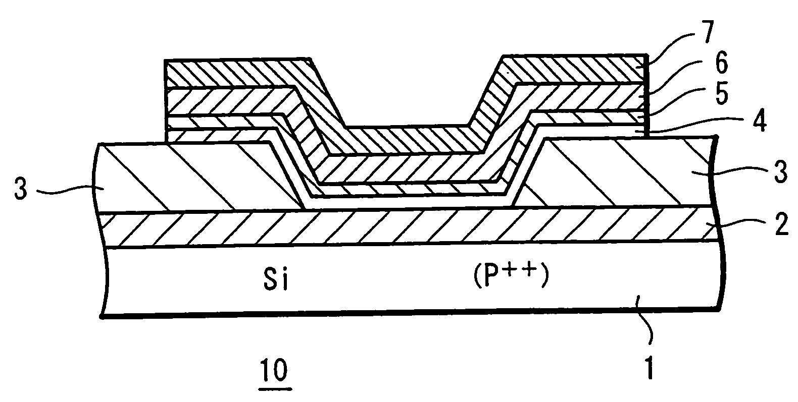
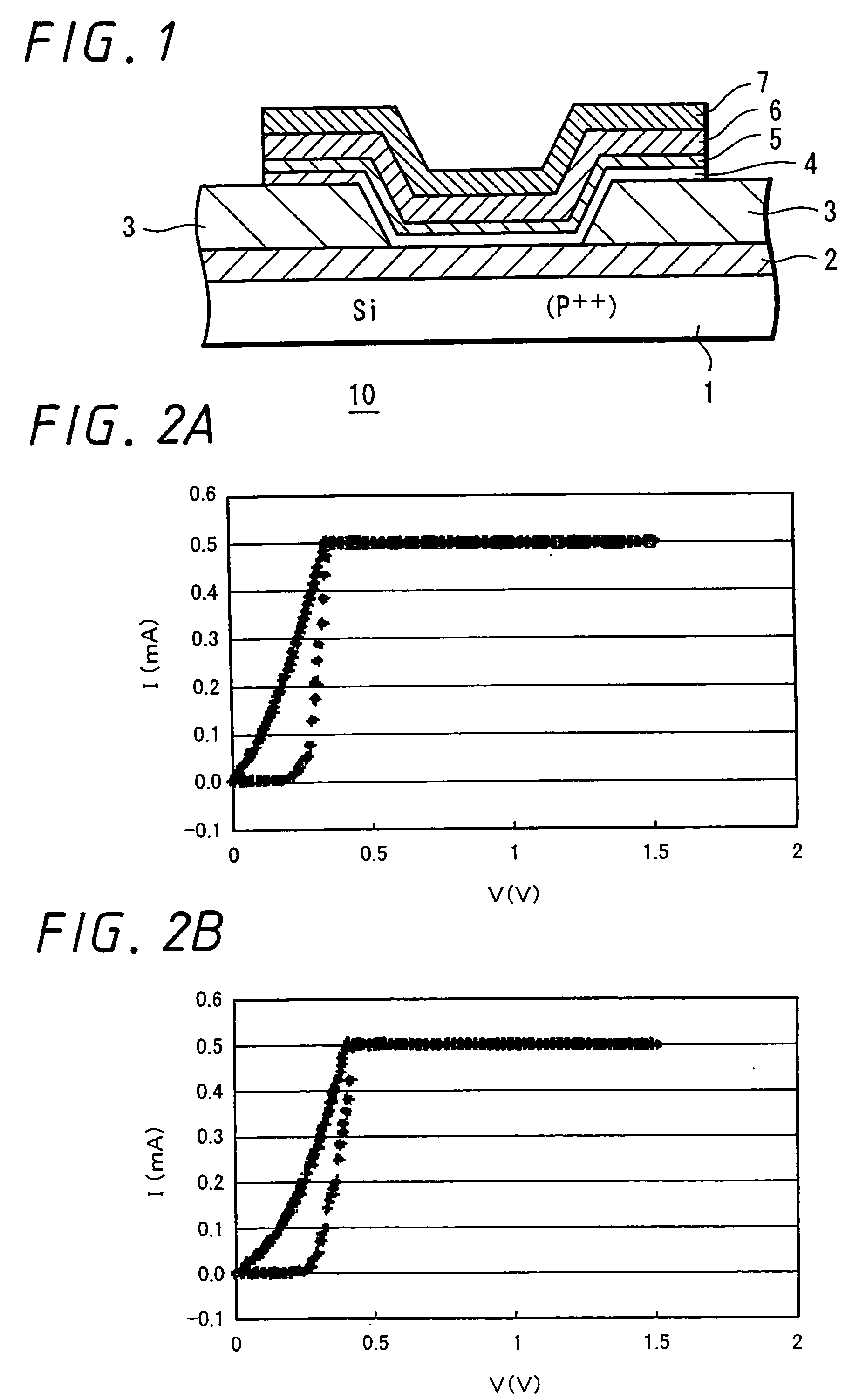
[0071]FIG. 1 shows a schematic constitutional view (a vertical section) as an embodiment of a memory element according to the present invention.

[0072] An memory element 10 is composed of a lower electrode 2 formed on a substrate 1 with a high electric conductivity, for example, on a (P++) silicon substrate which is doped with a p-type impurity of high density and a multi-layered coating including an amorphous thin-film 4, an upper electrode 5, an electrode layer 6 and a conductive layer 7 formed to connect to the lower electrode 2 through an opening formed in an insulating film 3 on the lower electrode 2.

[0073] For example, TiW, Ti and W can be used for the lower electrode 2.

[0074] In the case where TiW is used for the lower electrode 2 for example, the coating thickness may be set in the range of 20 nm to 100 nm, for example.

[0075] For example, a photo-resist with the hard cure treatment, SiO2 and Si3N4 conventionally used for a semiconductor device and other materials, for exa...


PUM


Abstract

A memory element in which recording and reading-out of information can easily be performed and which can be manufactured easily using a comparatively simple manufacturing method and a storage device using the memory element are provided.
A memory element 10 includes an amorphous thin-film 4 that is in between a first electrode 2 and a second electrode 5, in which at least one electrode in the first electrode 2 and the second electrode 5 contains Ag or Cu and the amorphous thin-film 4 is composed of Ge, and at least one element selected from S, Se, Te and Sb. Also a storage device includes the memory element 10, a wiring connected to the side of the first electrode 2 and a wiring connected to the side of the second electrode 5, in which a memory element 10 is arranged in large numbers.

Description

TECHNICAL FIELD [0001] The present invention relates to a memory element in which information is recorded and a storage device using the memory element. BACKGROUND ART [0002] In information equipment such as a computer, DRAM of high speed operation and high density is widely used as a random access memory. [0003] However, a production cost of DRAM is high in comparison with a conventional logic circuit LSI and signal processor that are used for electric equipment, because the manufacturing process is complicated. [0004] Also, DRAM is a volatile memory that information disappears when the power supply is cut off, and needs a refresh operation frequently, namely an operation that the read-in information is read out and is amplified again and is read again. [0005] Therefore, FeRAM (Ferroelectric Random Access Memory) and MRAM (Magnetic Random Access memory) and others are proposed for example, as a non-volatile memory that information does not disappear when the power supply is cut off...

Claims


Application Information

Patent Timeline
IPC IPC(8): H01L45/00
CPCH01L45/145H01L45/085H01L45/1233H01L45/1625H01L45/144H01L45/146H01L45/1266H10N70/245H10N70/8416H10N70/883H10N70/026H10N70/826H10N70/8828H10N70/8833H01L27/10
Inventor ARATANI, KATSUHISAKOUCHIYAMA, AKIRAISHIDA, MINORU
Owner SONY CORP
Why Eureka
Try Eureka