In-situ surface treatment for memory cell formation

a memory cell and surface treatment technology, applied in the field of semiconductor fabrication, can solve the problems of slowest than other types of storage devices, volatile memory cells usually lose their information, and silicon-based devices are approaching their fundamental physical size limits, so as to reduce the drawbacks inherent in conventional inorganic memory, limit device performance capabilities, and reduce the effect of density

Inactive Publication Date: 2005-10-13
CYPRESS SEMICON CORP
View PDF9 Cites 91 Cited by
  • Summary
  • Abstract
  • Description
  • Claims
  • Application Information

AI Technical Summary

Benefits of technology

[0010] The following presents a simplified summary of the invention in order to provide a basic understanding of some aspects of the invention. This summary is not an extensive overview of the invention. It is intended to neither identify key or critical elements of the invention nor delineate the scope of the invention. Its purpose is merely to present some concepts of the invention in a simplified form as a prelude to the more detailed description that is presented later.
[0011] The present invention relates to systems and methodologies for forming organic memory cells, which mitigate drawbacks inherent in conventional inorganic memory devices, such as volatility, limited density and limited device performance capabilities, for example. In according with one or more aspects of the present invention, a portion of an organic memory cell known as a passive layer is formed out of and atop an underlying conductive layer via treatment with plasma. Such a passive layer generally includes a conductivity facilitating compound, such as copper sulfide (Cu2S), which can be formed out of the conductive layer by treating an upper portion of the conductive layer with plasma, which can be generated from fluorine (F) based gases, for example. The conversion process can be monitored and controlled to facilitate, among other things, formation of the passive layer to a desired thickness, for example.

Problems solved by technology

Typically, in heat treatment operations, no additional material is added or removed from the wafer, although contaminates and vapors may evaporate from the wafer.
The long term storage mediums typically store larger amounts of information at a lower cost, but are slower than other types of storage devices.
Volatile memory cells usually lose their information if they lose power and typically require periodic refresh cycles to maintain their information.
However, silicon-based devices are approaching their fundamental physical size limits.
Inorganic solid state devices are generally encumbered with a complex architecture which leads to high cost and a loss of data storage density.
The volatile semiconductor memories based on inorganic semiconductor material require a near constant supply of electric current, which produces heating and high electric power consumption in order to merely maintain stored information.
However, non-volatile semiconductor memory cells have a reduced data rate, high power consumption and a large degree of complexity as compared with typical volatile memory cells.
Further, as the size of inorganic solid state devices decreases and integration increases, sensitivity to alignment tolerances can also increase making fabrication markedly more difficult.
Thus, further device shrinking and density increasing may be limited for inorganic memory cells.
Furthermore, such shrinkage for inorganic non-volatile memory cells, while meeting increased performance demands, is particularly difficult to do while maintaining low costs.

Method used


Image

  • In-situ surface treatment for memory cell formation
  • In-situ surface treatment for memory cell formation
  • In-situ surface treatment for memory cell formation

Examples


Embodiment Construction

[0035] The present invention is now described with reference to the drawings, wherein like reference numerals are used to refer to like elements throughout. In the following description, for purposes of explanation, numerous specific details are set forth in order to provide a thorough understanding of the present invention. It may be evident, however, to one skilled in the art that one or more aspects of the present invention may be practiced with a lesser degree of these specific details. In other instances, known structures and devices may be shown in block diagram form in order to facilitate describing one or more aspects of the present invention.

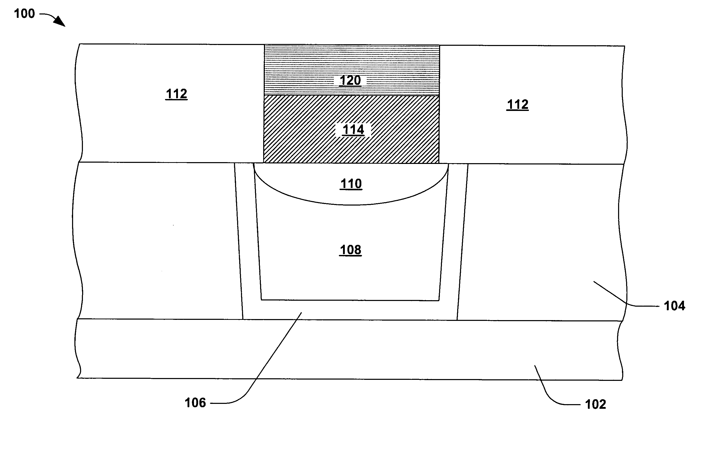
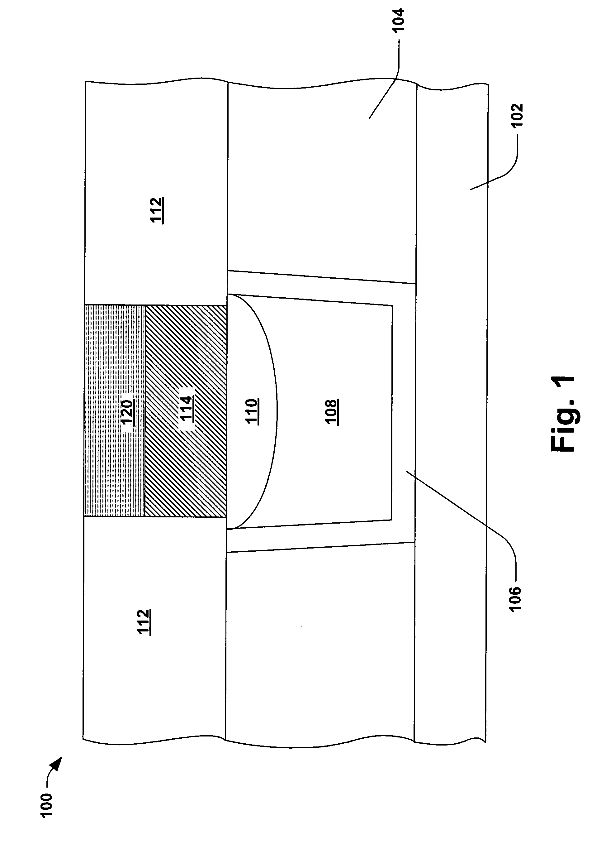
[0036]FIG. 1 is a cross sectional illustration of an organic memory cell 100, a portion of which can be formed according to one or more aspects of the present invention. Organic memory cells are memory devices that are, at least partly, based on organic materials and, are thus able to overcome some of the limitations of inorganic based...


PUM

PropertyMeasurementUnit
thicknessaaaaaaaaaa
thicknessaaaaaaaaaa
thicknessaaaaaaaaaa

Abstract

A system and methodology are disclosed for forming a passive layer on a conductive layer, such as can be done during fabrication of an organic memory cell, which generally mitigates drawbacks inherent in conventional inorganic memory devices. The passive layer includes a conductivity facilitating compound, such as copper sulfide (Cu2S), which is generated from an upper portion of a conductive material. The conductive material can serve as a bottom electrode in the memory cell, and the upper portion of the conductive material can be transformed into the passive layer via treatment with a plasma generated from fluorine (F) based gases.

Description

FIELD OF INVENTION [0001] The present invention relates generally semiconductor fabrication and, in particular, to a system and methodology for forming a conductivity facilitating layer for an organic memory cell via plasma treatment. BACKGROUND OF THE INVENTION [0002] In the semiconductor industry there is a continuing trend toward increasing device densities, throughput and yield. To increase device densities there have been, and continue to be, efforts toward scaling down semiconductor device dimensions (e.g., at sub-micron levels). In order to accomplish such densities, smaller feature sizes and more precise feature shapes are required. This may include the width and spacing of interconnecting lines, spacing and diameter of contact holes, and the surface geometry, such as comers and edges, of various features. To increase throughput, the number of required processing steps can be reduced and / or the time required for those processing steps can be reduced. To increase yield, which...

Claims


Application Information

Patent Timeline
Patent Type & Authority Applications(United States)
IPC IPC(8): H01L21/00H01L21/311
CPCH01L21/67069H01L21/311H01L21/00
Inventor HUI, ANGELA T.
Owner CYPRESS SEMICON CORP
Why Eureka
Try Eureka