Supercharge Your Innovation With Domain-Expert AI Agents!

Cutting thin layer(s) from semiconductor material(s)

a technology of semiconductor materials and thin layers, applied in the direction of manufacturing tools, welding/soldering/cutting articles, metal working apparatuses, etc., can solve the problems of consuming and sacrificing substrates, high resistance substrates not necessarily available at the same cost and quality, and thinning techniques based on mechanical, chemical,

Inactive Publication Date: 2005-10-13
SOITEC SA
View PDF6 Cites 3 Cited by
  • Summary
  • Abstract
  • Description
  • Claims
  • Application Information

AI Technical Summary

Benefits of technology

The present invention provides a new method of cutting a semiconductor material along a zone of weakness without raising temperature, chemical etching, or decomposing the layer of weakness. This method involves injecting a pulse of energy into the substrate where the layer of weakness is located. The energy pulse is directed to cause cleavage in the weakened zone. The method can be used to make electronic, optoelectronic, or optical components or sensors by cutting thin layers from a substrate or ingot forming element. The apparatus for carrying out this method includes means for generating and directing a pulse of energy, which can be a laser or a sheet of solid lasers or a pulsed diode type pulse accelerator. The technical effects of this invention include improved precision and efficiency in cutting semiconductor materials, as well as reduced damage to the substrate and improved quality of the resulting components or sensors.

Problems solved by technology

Typically, the insulator used is SiO2 of amorphous structure on which it is not possible to deposit silicon of monocrystalline quality.
However a highly resistive substrate is not necessarily available at the same cost and quality as the standard substrates that are usually used.
Techniques based on thinning down (mechanically, chemically, etc.) suffer from the drawback of consuming and sacrificing a substrate, which is inefficient from an economic standpoint.
Such thinning techniques are also often quite difficult and expensive to implement.
Combinations based on applying external mechanical stresses (shear, twisting, bending, tension, and the like) suffer from the drawback of generally requiring adhesion (molecular or otherwise) that is sufficiently strong to avoid breaking under the stress needed for rupturing the weak zone.
A method for obtaining such adhesion is not always available in certain manufacturing methods or applications which are subject to very severe specifications (e.g., where it is impossible to heat, impossible to use specific solvents or other chemicals, impossible to apply traction to the structure because of the risk of destroying sensitive components, etc.).
For example, the new support may not be capable of withstanding the temperatures required.
By way of another example, the incompatibility can stem from the combination of materials, in particular because they have too great a difference in thermal expansion coefficients which would cause an assembly that is not sufficiently uniform to break during a temperature rise.
Techniques based on chemical etching are aggressive and this can make them incompatible with the final support on which the layer for transfer is to be integrated, or with components that might already be present on that layer.
The authors also state that that method of implementation requiring relatively large amounts of energy to be delivered in order to operate suffers from the drawback of possibly damaging the layer that is to be transferred.

Method used


Image

  • Cutting thin layer(s) from semiconductor material(s)
  • Cutting thin layer(s) from semiconductor material(s)
  • Cutting thin layer(s) from semiconductor material(s)

Examples


Embodiment Construction

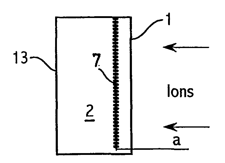
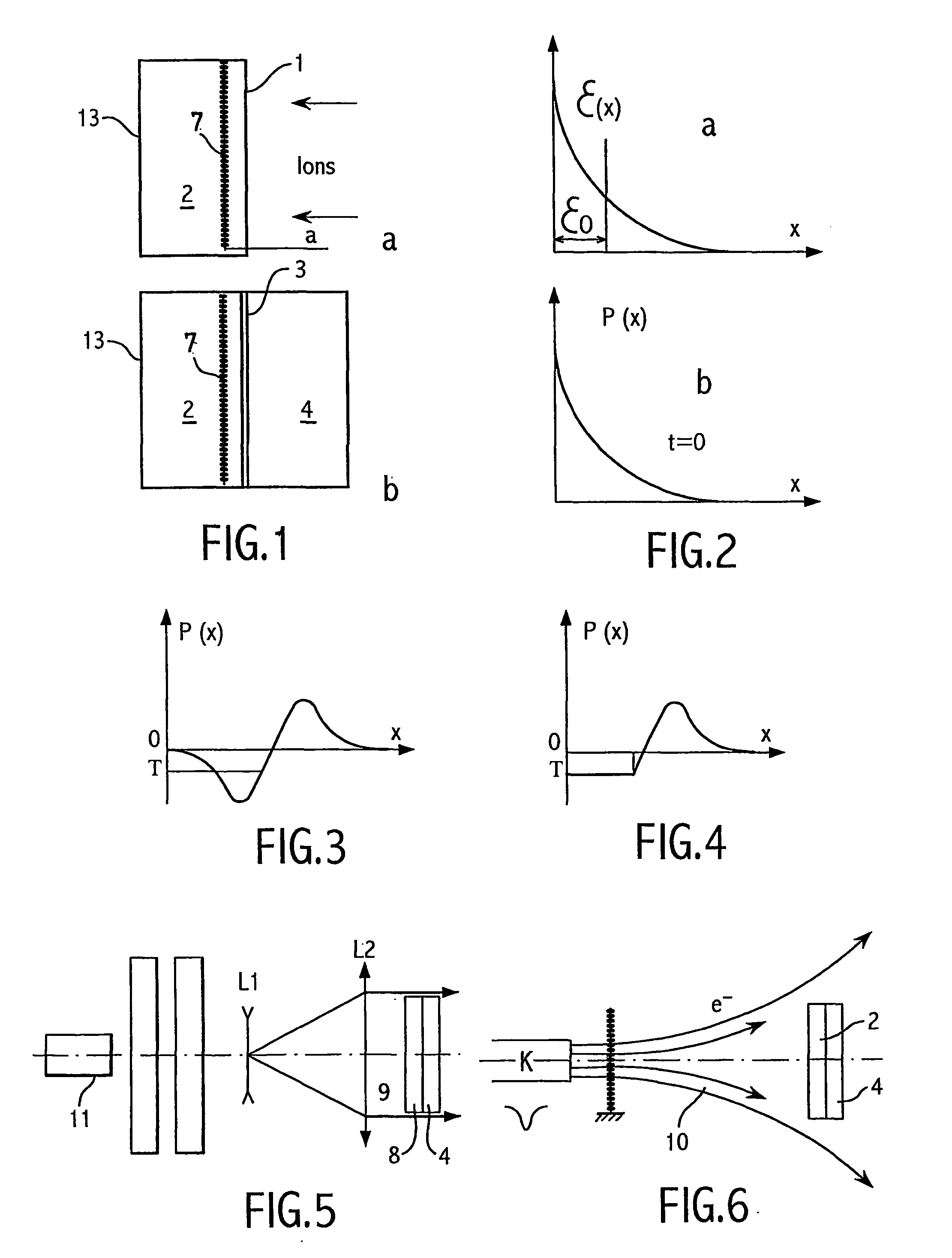
[0042] In a preferred first implementation of the invention, the procedure is as follows. The starting material is a semiconductor wafer, e.g. of silicon 2 (see FIG. 1) having a thickness of about 500 μm, which is polished on one of its faces 1. Protons are implanted in its face at an energy such that their penetration depth into the semiconductor is a little greater than the thickness λ of the thin layer of semiconductor that is to be made. For example, to make a layer that is about 1 μm thick, protons are used at an energy of about 150 kilo-electon volts (keV).

[0043] Thereafter, an insulating substrate 4 is prepared, and in the example shown in FIG. 1 this is a substrate of silicon covered in a layer of SiO2 having a typical thickness of a few tenths of a micrometer.

[0044] Thereafter, the substrates (4 and 2) are bonded together by molecular adhesion using a method that is now well known (see for example the text “Semiconductor wafer bonding Science and Technology” by Q. Y. Tong...


PUM

PropertyMeasurementUnit
diameteraaaaaaaaaa
diameteraaaaaaaaaa
resistivitiesaaaaaaaaaa

Abstract

An apparatus for cutting at least one thin layer from a substrate or ingot forming element for an electronic or optoelectronic or optical component or sensor. This apparatus includes a device for directing a pulse of energy into the substrate or forming element wherein the pulse has a duration shorter than or of the same order as that needed by a sound wave to pass through the thickness of the weakened zone, and the energy of the pulse is sufficient to cause cleavage to take place in the weakened zone as the energy of the pulse is absorbed therein. The apparatus also includes an assembly for holding or orienting the substrate or ingot forming element so that the energy pulse is completely uniformly directed over the entire surface, through the face and into the substrate or ingot forming element to cause cleavage to take place in the weakened zone as the energy of the pulse is absorbed therein.

Description

CROSS-REFERENCE TO RELATED APPLICATIONS [0001] This application is a division of application Ser. No. 10 / 268,776 filed Oct. 11, 2002, now U.S. Pat. No. ______, which is a continuation of International application no. PCT / FR01 / 01179 filed Apr. 17, 2001, the entire content of each of which is expressly incorporated herein by reference thereto.BACKGROUND ART [0002] The invention relates to cutting at least one thin layer from a substrate or ingot, in particular of semiconductor material(s), for making an electronic, optoelectronic or optical component or sensor. [0003] In numerous applications associated with the fields of microelectronics, optoelectronics, and sensors, the technological operation of transferring a layer of one substrate onto another represents a key operation that enables numerous materials structures or specific components to be fabricated. The layer for transfer may or may not include components that are complete or in a partial state of completion. [0004] One examp...

Claims


Application Information

Patent Timeline
Patent Type & Authority Applications(United States)
IPC IPC(8): H01L21/304B23K26/40H01L21/301H01L21/762
CPCB23K26/407B23K26/4075H01L21/76254B23K2201/40B23K26/4085B23K26/40B23K2101/40B23K2103/16B23K2103/50B82Y30/00H01L21/30
Inventor ROCHE
Owner SOITEC SA
Features
  • R&D
  • Intellectual Property
  • Life Sciences
  • Materials
  • Tech Scout
  • Unparalleled Data Quality
  • Higher Quality Content
  • 60% Fewer Hallucinations
Learn More