Coupling structure of electronic components

Inactive Publication Date: 2005-10-20
SHARP KK
View PDF5 Cites 9 Cited by
  • Summary
  • Abstract
  • Description
  • Claims
  • Application Information

AI Technical Summary

Benefits of technology

[0024] The present invention was done to solve the above-described problem. The objective of the present invention is therefore to realize a coupling structure

Problems solved by technology

If moisture or dust is adhered to this exposed part, short-circuit or leakage failure may occur.
On account of this structure, ion migration is induced by adhered moisture, thereby causing short-circuit and leakage failure.
In this case, the rel

Method used


Image

  • Coupling structure of electronic components
  • Coupling structure of electronic components
  • Coupling structure of electronic components

Examples


Embodiment Construction

[0043] The following will discuss an embodiment of the present invention in reference to FIGS. 1 through 6. The present embodiment illustrates a coupling structure of a liquid crystal driver and a liquid crystal panel of a liquid crystal display device, but the present invention is not limited to this embodiment.

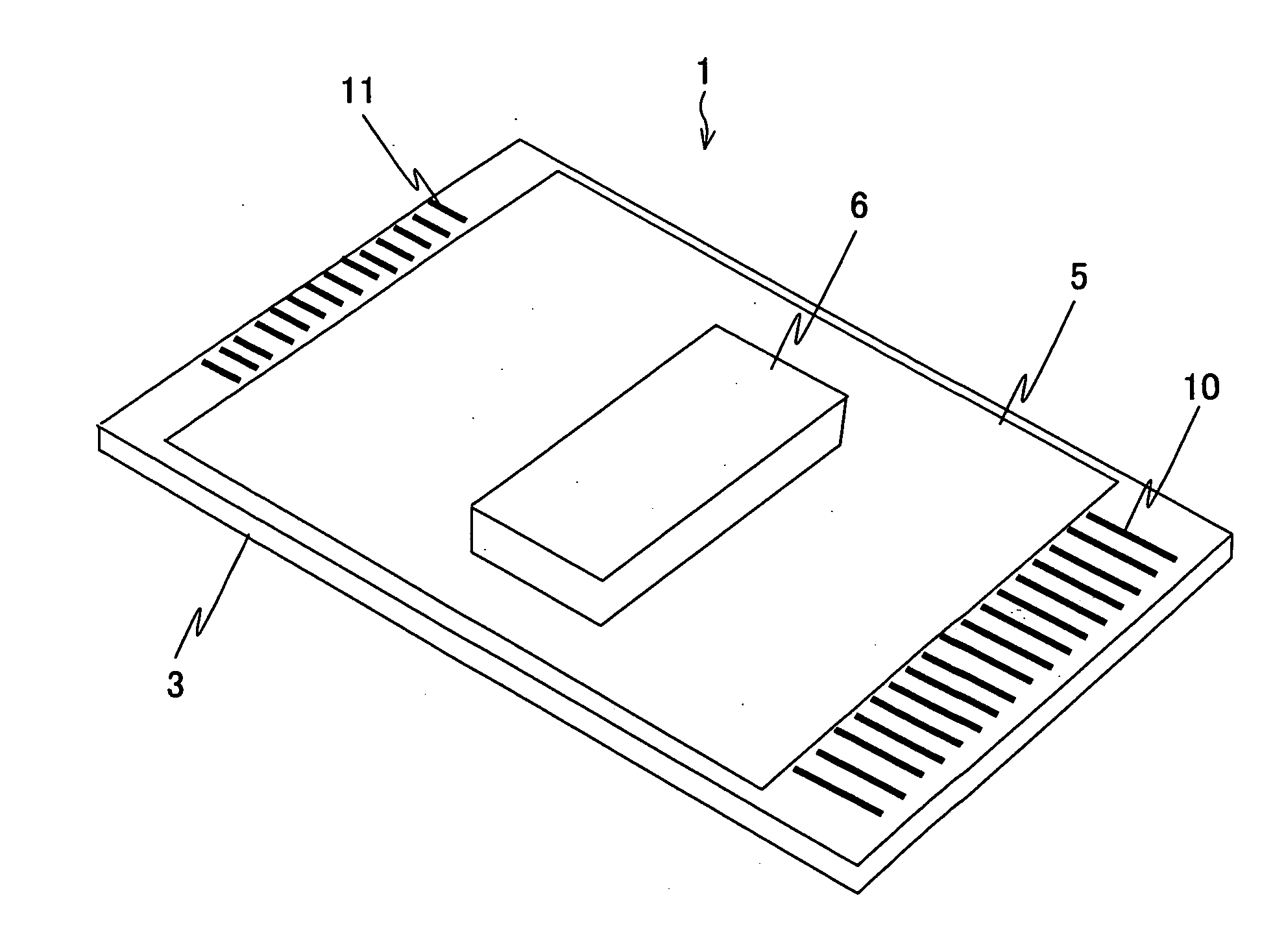
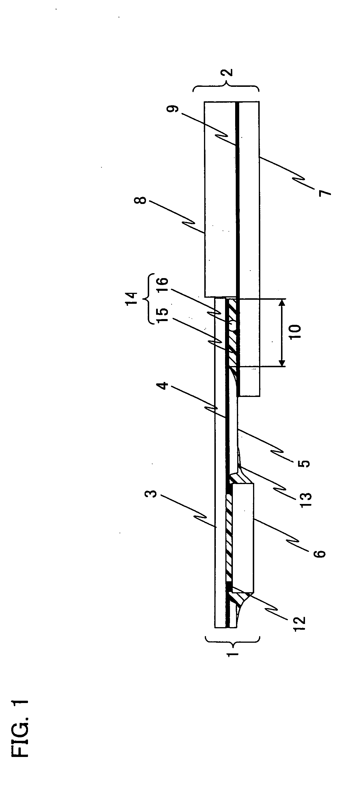
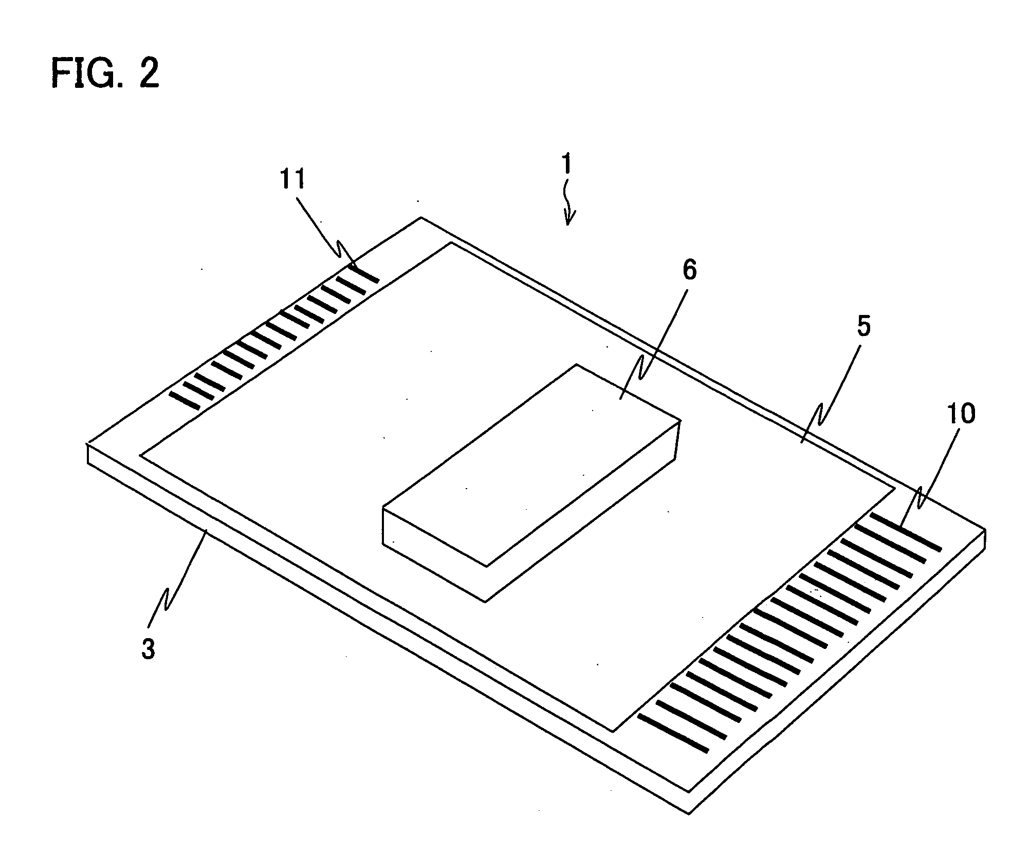
[0044]FIG. 1 is a cross section schematically showing a coupling structure of a liquid crystal driver (first electronic component) and a liquid crystal panel (second electronic component) of the present embodiment. FIG. 2 is an oblique perspective view showing schematic arrangement of the liquid crystal driver 1. As FIGS. 1 and 2 show, the liquid crystal driver 1 includes a flexible substrate (first substrate) 3, drive wiring (first wiring) 4, a solder resist (protective film) 5, and a driver chip 6. The liquid crystal panel 2 includes an element substrate (second substrate) 7, an opposing substrate (third substrate) 8, and display wiring (second wiring) 9.

[0045] The flexi...


PUM


Abstract

A coupling structure of electronic components, by which the break down of drive wiring at the time of folding a flexible substrate is prevented and the reliability of wiring is increased, is realized. In the coupling structure of electronic components of the present invention, a liquid crystal driver and a liquid crystal panel are arranged such that a surface of the flexible substrate, that surface being provided with the drive wiring and a solder resist, faces a surface of an element substrate, that surface being provided with display wiring. Furthermore, the drive wiring and the display wiring are electrically coupled to each other, and the solder resist is in contact with the element substrate.

Description

[0001] This Nonprovisional application claims priority under 35 U.S.C. § 119(a) on patent application No. 2004-123133 filed in Japan on Apr. 19, 2004, the entire contents of which are hereby incorporated by reference. FIELD OF THE INVENTION [0002] The present invention relates to a coupling structure of electronic components. More specifically, the present invention relates to a coupling structure that allows a liquid crystal driver and a liquid crystal panel to be electrically coupled to each other. BACKGROUND OF THE INVENTION [0003] A liquid crystal display device has conventionally been used as a COF (Chip On Film) module device. Such a liquid crystal display device includes: a liquid crystal driver including a flexible substrate on which a driver chip for driving elements of a liquid crystal panel is provided; and the liquid crystal panel including an element substrate and an opposing substrate. The liquid crystal driver and the liquid crystal panel are electrically coupled to e...

Claims


Application Information

Patent Timeline
IPC IPC(8): G02F1/13H01R11/01G02F1/1345H01R12/00H05K1/00H05K1/14H05K3/28H05K3/32H05K3/36
CPCG02F1/13452H01R12/61H05K2201/2036H05K3/323H05K3/361H05K3/28G02F1/1345
Inventor NAITOH, KATSUYUKITOYOSAWA, KENJI
Owner SHARP KK
Why Eureka
Try Eureka