Triode type field emission display with high resolution

a field emission display and high resolution technology, applied in the field of high-resolution field emission display, can solve the problems of failure of space revolution, diode type structure is unsuitable for applications requiring high-resolution displays, etc., and achieves improved electron emission efficiency, high resolution, and good display quality.

Active Publication Date: 2005-10-27
HON HAI PRECISION IND CO LTD +1
View PDF10 Cites 10 Cited by
  • Summary
  • Abstract
  • Description
  • Claims
  • Application Information

AI Technical Summary

Benefits of technology

[0011] Accordingly, an object of the present invention is to provide a triode type field emission display which has an improved efficiency of electron emission, by emitting electrons at a relative low voltage, and by focusing the emitted electrons to a desired picture element effectively.
[0012] Another object of the present invention is to provide a triode type field emission display which has high resolution and good display quality.

Problems solved by technology

Diode type structures are unsuitable for applications requiring high resolution displays, because the diode type structures require high voltages, produce relatively non-uniform electron emissions, and require relatively costly driving circuits.
Also, if electrons arrive at fluorescent material 107 of a neighboring red-color's picture element, then a failure in space revolution occurs.

Method used


Image

  • Triode type field emission display with high resolution
  • Triode type field emission display with high resolution
  • Triode type field emission display with high resolution

Examples


Embodiment Construction

[0027] Reference will now be made to the drawings to describe a preferred embodiment of the present invention in detail.

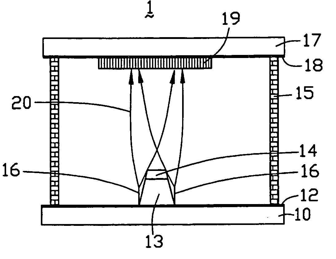
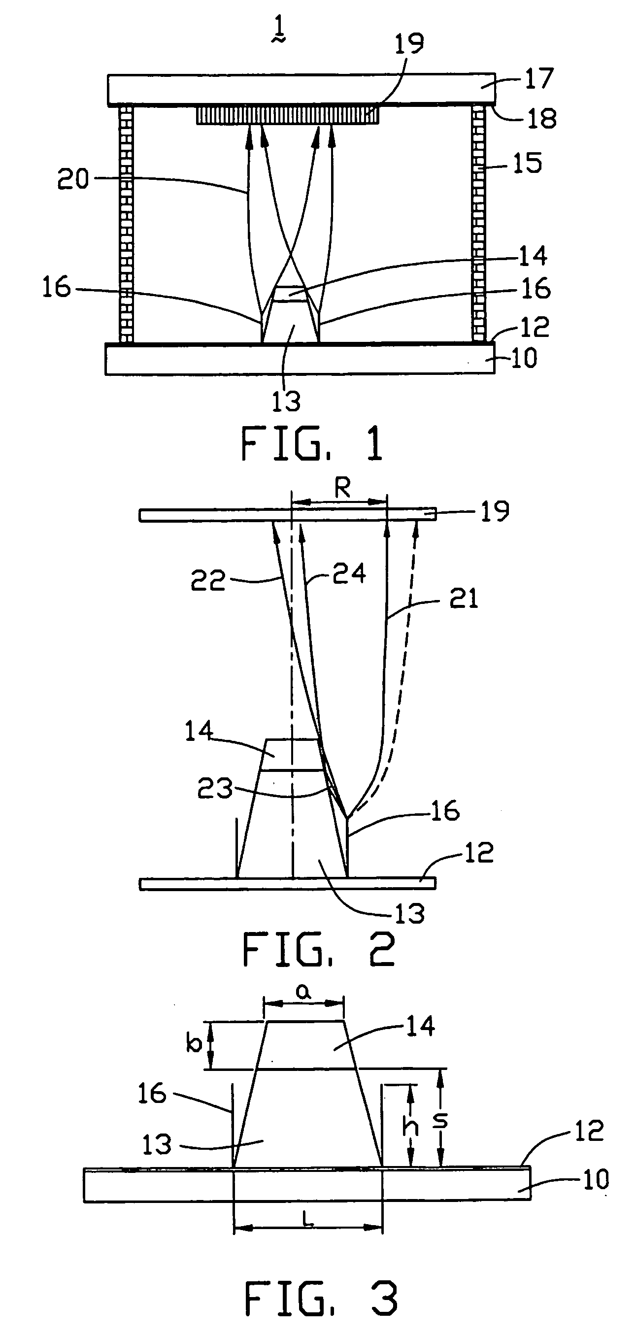
[0028] Referring initially to FIG. 1, one picture element or display pixel unit of a carbon nanotube-based field emission display 1 in accordance with a preferred embodiment of the present invention comprises: a cathode electrode 12 which is formed on an insulation substrate 10; an insulation layer 13 made of an insulative material disposed on the cathode electrode 12 and covering only a part of the cathode electrode 12; a gate electrode 14 made of a metallic material (preferred metal with excellent electrical conductivity) formed on a top of the insulation layer 13; a plurality of carbon nanotubes 16 (only two are shown in the FIG. 1) functioning as electron emitters for emitting electrons formed on portions of the cathode electrode 12 adjacent to two sides of the insulation layer 13; an anode electrode 18 made of an indium-tin-oxide (ITO) thin film formed on a s...


PUM


Abstract

A triode type field emission display in accordance with the invention includes: a cathode electrode (12) formed on an insulation substrate (10); an insulation layer (13) formed on the cathode electrode; a gate electrode (14) formed on the insulation layer; a number of emitters (16); and an anode electrode (18) with a phosphor layer (19) positioned over the gate electrode. The emitters are distributed on portions of the cathode electrode at two sides of the insulation layer, and a height of the emitters is less than a thickness of the insulation layer. The emitters are capable of emitting electrons from tips thereof, and the emitted electrons are focused on the phosphor layer by an electric field generated by the gate electrode.

Description

BACKGROUND OF THE INVENTION [0001] 1. Field of the Invention [0002] The present invention relates to a field emission device and more particularly to a high-resolution field emission display having a three-electrode structure of a cathode, an anode and a gate electrode. [0003] 2. Prior Art [0004] Field emission displays (FEDs) are new, rapidly developing flat panel display technologies. Compared to conventional technologies, e.g., cathode-ray tube (CRT) and liquid crystal display (LCD) technologies, FEDs are superior in having a wider viewing angle, low energy consumption, a smaller size and a higher quality display. In particular, carbon nanotube-based FEDs (CNTFEDs) have attracted much attention in recent years. [0005] Carbon nanotube-based FEDs employ carbon nanotubes (CNTs) as electron emitters. Carbon nanotubes are very small tube-shaped structures essentially having a composition of a graphite sheet rolled into a tube. Carbon nanotubes produced by arc discharge between graphit...

Claims


Application Information

Patent Timeline
Patent Type & Authority Applications(United States)
IPC IPC(8): H01J1/62H01J3/02H01J31/12
CPCH01J31/123H01J3/022
Inventor WEI, YANGFAN, SHOU-SHAN
Owner HON HAI PRECISION IND CO LTD
Why Eureka
Try Eureka