Imaging apparatus for small spot optical characterization

Inactive Publication Date: 2005-10-27
SCHNITTKER MARK VICTOR
View PDF7 Cites 3 Cited by
  • Summary
  • Abstract
  • Description
  • Claims
  • Application Information

AI Technical Summary

Benefits of technology

[0011] The primary object of the invention is to provide a simple low cost means of optical characterization on the micrometer scale.
[0012] Another object of the invention is to integrate a real time optical imager to ease the alignment of micrometer scale optical characterization.
[0016] In accordance with a preferred embodiment of the invention, there is disclosed an imaging apparatus for small spot optical characterization comprising: an optical housing, a beam splitter, and a turn mirror assembly. Said optical housing provides a focal plane and an image plane confocal to each other. Said turn mirror assembly integrates a reflective surface, aperture, airspace waveguide, and an optical port. The aperture integrated into the turn mirror assembly greatly simplifies the design while illumination incident on the aperture provides a projection of the optical port onto the surface of the object. The projected image of the optical port onto the object creates a dark target, which is viewable at the image plane using a low cost CCD camera. The field of view of the CCD camera is large compared to that of the optical port, but is spectrally narrow. The large field of view allows for real time alignment of the projected optical port onto the sample. The aperture is located at the focal plane. The aperture and optical port are joined with the airspace waveguide. Because of the aperture, the optical port has a narrow field of view compared to that of the CCD image. Because the optical path from the objective lens to the optical port is entirely reflective, the optical port has functionality over a wide spectral range.

Problems solved by technology

As the measurement area reduces, the challenge of optical characterization becomes more difficult.
The complexity of their design increases cost beyond what is justified for simple optical characterization in semiconductor processes.
Furthermore, their physical size is generally too large to mount into existing equipment where space is of concern.
Infrared versions of these microscopes that use thermal or near infrared 2D imagers also suffer from reduced resolution due to the low pixel density of current technologies.
The combination of size and cost yield complex microscope designs impractical to implement on a large scale.
Non-imaging optical assemblies designed for optical characterization are small, simple and low cost but make it difficult to target the optical system onto a small well defined position.
Supplementing the system with a microscope mounted at an angle relative to the assembly can reduce this issue, but suffers from parallax in systems that do not project a beam of light onto the surface of the sample.
Furthermore, non-imaging systems have no feedback to the user of their focus.
Because of the focus and alignment uncertainty, the chances of obtaining poor data are increased.
Many of the non-imaging configurations also have very short working distances, which prohibit their use in applications that have obstructions.
The increased challenge of robustly aligning non-imaging optical systems make them a poor choice for both production and failure analysis applications in the semiconductor industry.

Method used


Image

  • Imaging apparatus for small spot optical characterization
  • Imaging apparatus for small spot optical characterization
  • Imaging apparatus for small spot optical characterization

Examples


Embodiment Construction

[0021] Detailed descriptions of the preferred embodiment are provided herein. It is to be understood, however, that the present invention may be embodied in various forms. Therefore, specific details disclosed herein are not to be interpreted as limiting, but rather as a basis for the claims and as a representative basis for teaching one skilled in the art to employ the present invention in virtually any appropriately detailed system, structure or manner.

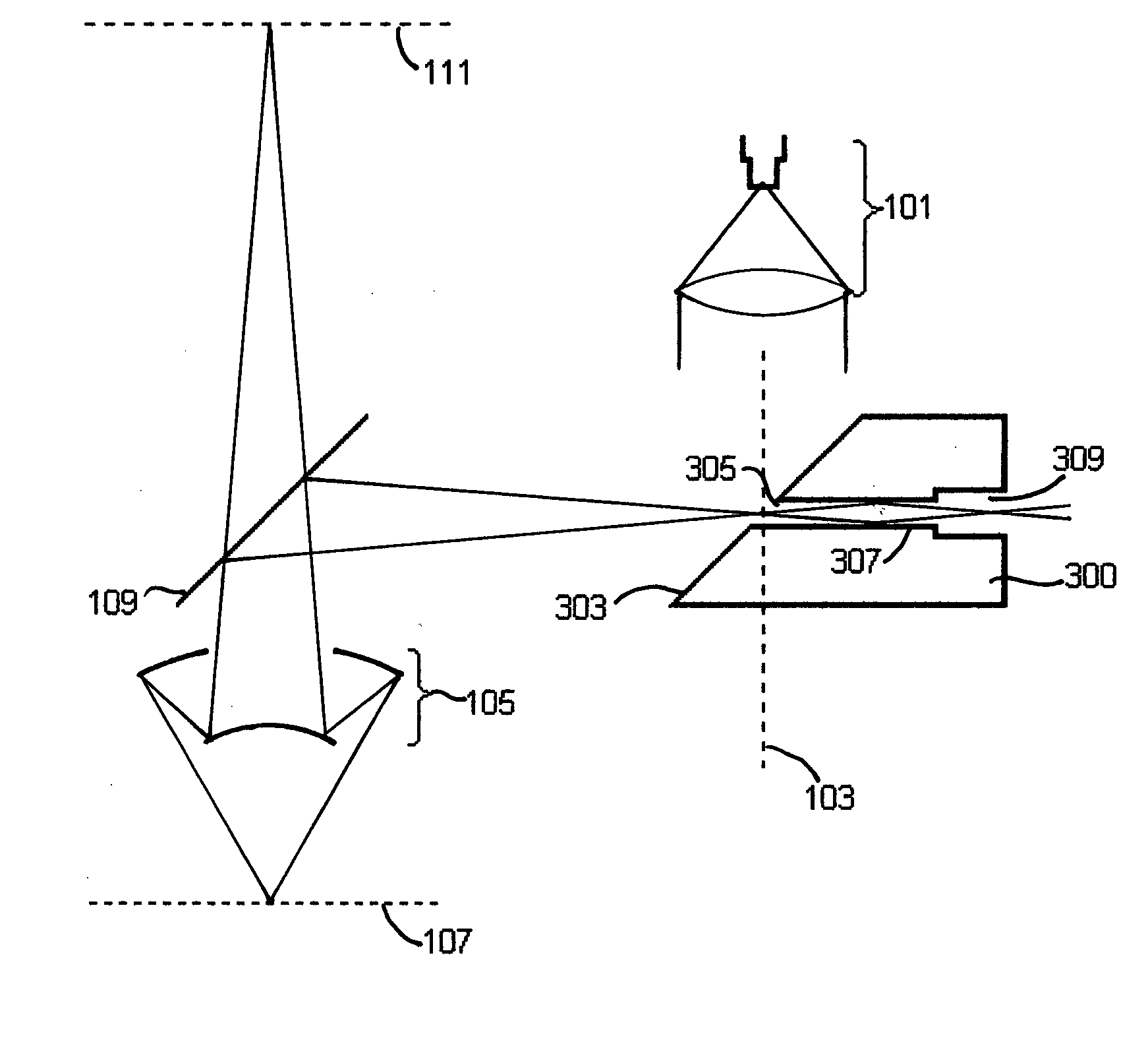
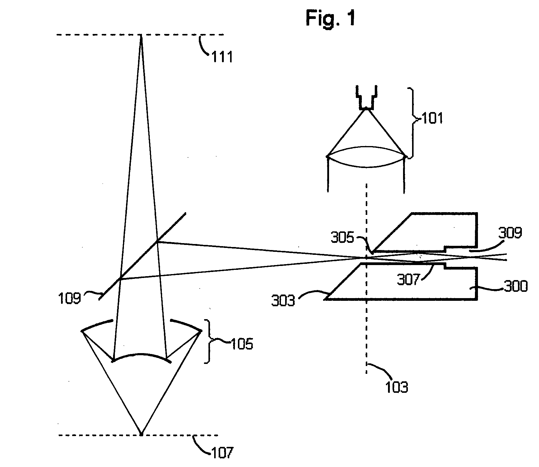
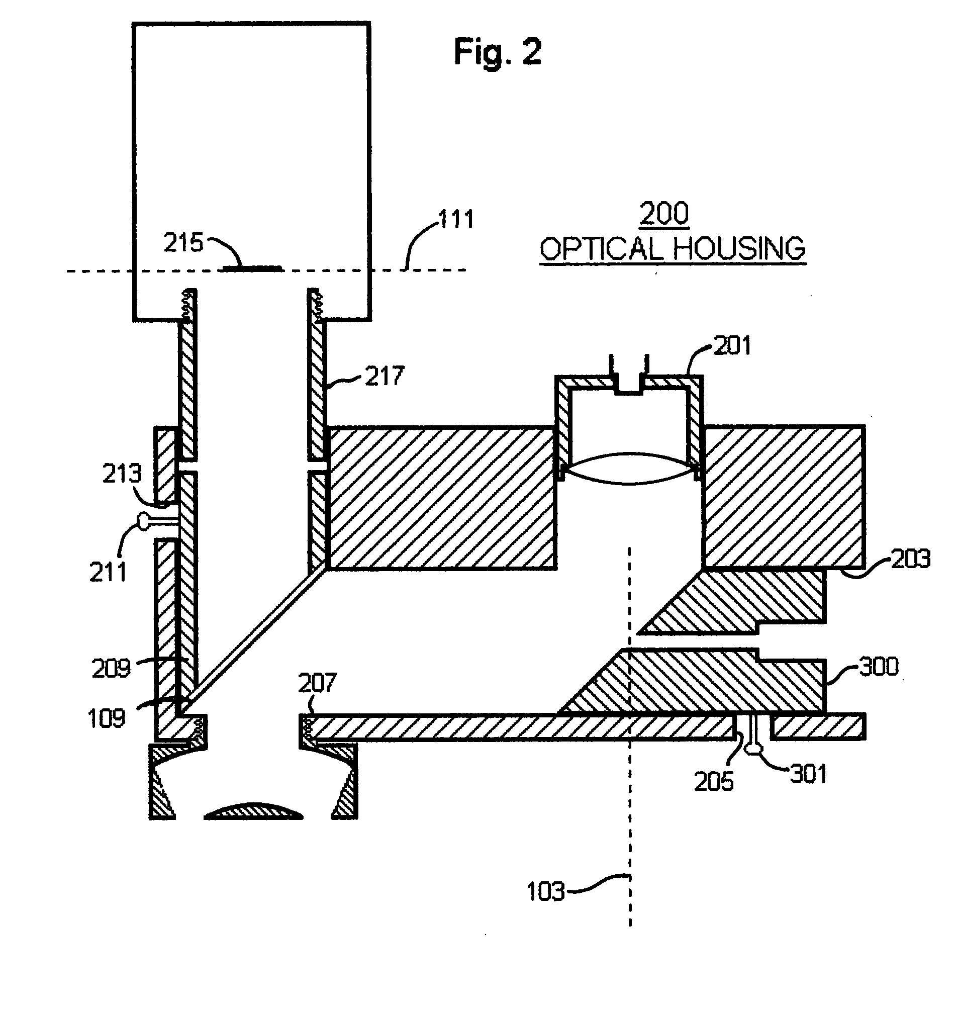
[0022]FIG. 1 is a schematic diagram of an imaging apparatus for small spot optical characterization in accordance with the present invention. The apparatus has accommodations for illumination from a near collimated light source 101. The light from the light source 101 illuminates the reflective surface 303 of the turn mirror assembly 300. The center of the reflective surface 303 is located at the focal plane 103. Light incident on the reflective surface 303 is reflected and turned in all areas except that of the location of the ape...


PUM


Abstract

An imaging tool which has an objective lens, a beam splitting mirror and a turning mirror. The turning mirror has a centrally integrated aperture. The turning mirror is located at a secondary focal plane in the illumination path, and thus there is no illumination at any point on the object pane which is stigmatic with the integrated aperture. The integrated aperture provides a means to inject or remove light from a small spatial portion of the object plane. An airspace waveguide is integrated into the metal substrate of the turning mirror and eases the transfer of light from an external optical port to and from the aperture, and then onto the object plane.

Description

CROSS REFERENCE TO RELATED APPLICATIONS [0001] Not Applicable STATEMENT REGARDING FEDERALLY SPONSORED RESEARCH OR DEVELOPMENT [0002] Not Applicable DESCRIPTION OF ATTACHED APPENDIX [0003] Not Applicable BACKGROUND OF THE INVENTION [0004] This invention relates generally to the field of microscopy and more specifically to small spot optical characterization. [0005] Optical characterization of materials has long been a valuable tool across many fields. Non-contact thermometry, electroluminescense, fluorescence, reflectance, and transmittance are some common forms of optical characterization. These techniques are greatly diverse in geometry, optical materials and wavelength, but they share a common trend. As technologies shrink in their physical dimensions, there exists a need to make the same measurement in a smaller area. As the measurement area reduces, the challenge of optical characterization becomes more difficult. This trend is very noticeable in the semiconductor industries whe...

Claims


Application Information

Patent Timeline
IPC IPC(8): G01N21/55
CPCG01N21/55
Inventor SCHNITTKER, MARK VICTOR
Owner SCHNITTKER MARK VICTOR
Why Eureka
Try Eureka