Effective method to improve sub-micron color filter sensitivity

a color filter and effective technology, applied in the field of solid-state imaging devices, can solve the problems of image quality decline, long focal length is a big challenge to maintaining adequate sensor sensitivity, and the size and oval shape of the microlens can be difficult to reproduce, so as to achieve the effect of improving sensitivity and long focal length

Active Publication Date: 2005-11-03
TAIWAN SEMICON MFG CO LTD
View PDF32 Cites 77 Cited by
  • Summary
  • Abstract
  • Description
  • Claims
  • Application Information

AI Technical Summary

Benefits of technology

[0008] An objective of the present invention is to provide a microlens component in a CMOS image sensor that offers improved sensitivity in a device that has several metal (ILM) layers and requires a long focal length.
[0009] A further objective of the present invention is to provide a microlens component in a CMOS image sensor that offers improved sensitivity in a sub-micron device that has a pixel size smaller than about 5 microns.
[0010] A still further objective of the present invention is to provide a method of fabricating a CMOS image sensor having improved efficiency that is compatible with existing tools and materials and can be performed in a low cost manner.
[0014] A planar overcoat layer which is preferably comprised of the same transparent material as in the insulation layer is formed on the first microlens array. A post-exposure bake at 220° C. not only hardens the overcoat layer but also hardens the first microlens array. A second microlens array comprised of a plurality of second microlenses is fabricated on the overcoat layer by first patterning a positive tone photoresist, heating to reflow, and hardening with a 220° C. bake to form flat, convex shapes. A second microlens has a width that is essentially equal to the width of a first microlens. Moreover, there is a second microlens aligned over each first microlens. A second microlens preferably has a radius of curvature (H2) that is greater than H1. The larger radius of curvature provides for a shorter focal length and higher photon collection efficiency for a second microlens compared to a first microlens. Light that is efficiently collected by a second microlens is focused on a first microlens. The first microlens has a long focal length that is capable of focusing light through a light column within a thick lower stack of layers onto a photodiode.
[0015] The invention is also a microlens component of a CMOS image sensor with improved sensitivity that is formed on a lower stack of layers that includes a photodiode array on a substrate and a color filter layer as the top layer in the lower stack. The lower stack typically includes a interconnect structure on the substrate and an insulation layer formed on the insulation layer. The microlens component is comprised of a first microlens array formed above the color filter layer, a planar transparent overcoat layer on the first microlens array, and a second microlens array formed on the overcoat layer. Each of the plurality of microlenses in the first microlens array and in the second microlens array has a flat convex shape. An important feature is that the radius of curvature of a second microlens is greater that the radius of curvature of a first microlens. A light column is formed which involves a vertical arrangement of a photodiode, a color filter region, a first microlens, and a second microlens. Other intermediate layers described previously have a high transmittance to minimize loss of light intensity as light passes through the light column. Photon collection efficiency (ψ) of a microlens is expressed by the equation ψ=4PI×R2 where PI is the photorefractive index of a microlens and R is the radius of curvature.

Problems solved by technology

High sensitivity is an important characteristic for a CMOS image sensor since the image quality may suffer if sensitivity is not high enough.
The longer focal length is a big challenge to maintaining adequate sensor sensitivity.
Since the lower microlens array does not reside on a planar surface, the size and oval shape of the microlens can be difficult to reproduce.
In addition, the poly(vinylphenol) / diazonaphthoquinone diazide (DNQ) based photoresist that comprises the lower microlens has less suitable dissolution characteristics for patterning than a more common Novolak resin / DNQ photoresist.

Method used


Image

  • Effective method to improve sub-micron color filter sensitivity
  • Effective method to improve sub-micron color filter sensitivity
  • Effective method to improve sub-micron color filter sensitivity

Examples


Embodiment Construction

[0021] The present invention is a microlens component of a CMOS image sensor that provides improved sensitivity for sub-micron devices that have a pixel size of less than 5 microns. A process is also described for forming the improved CMOS image sensor. The drawings are provided by way of example and are not intended to limit the scope of the invention. Furthermore, the relative sizes of the various elements within the drawings are not necessarily drawn to size.

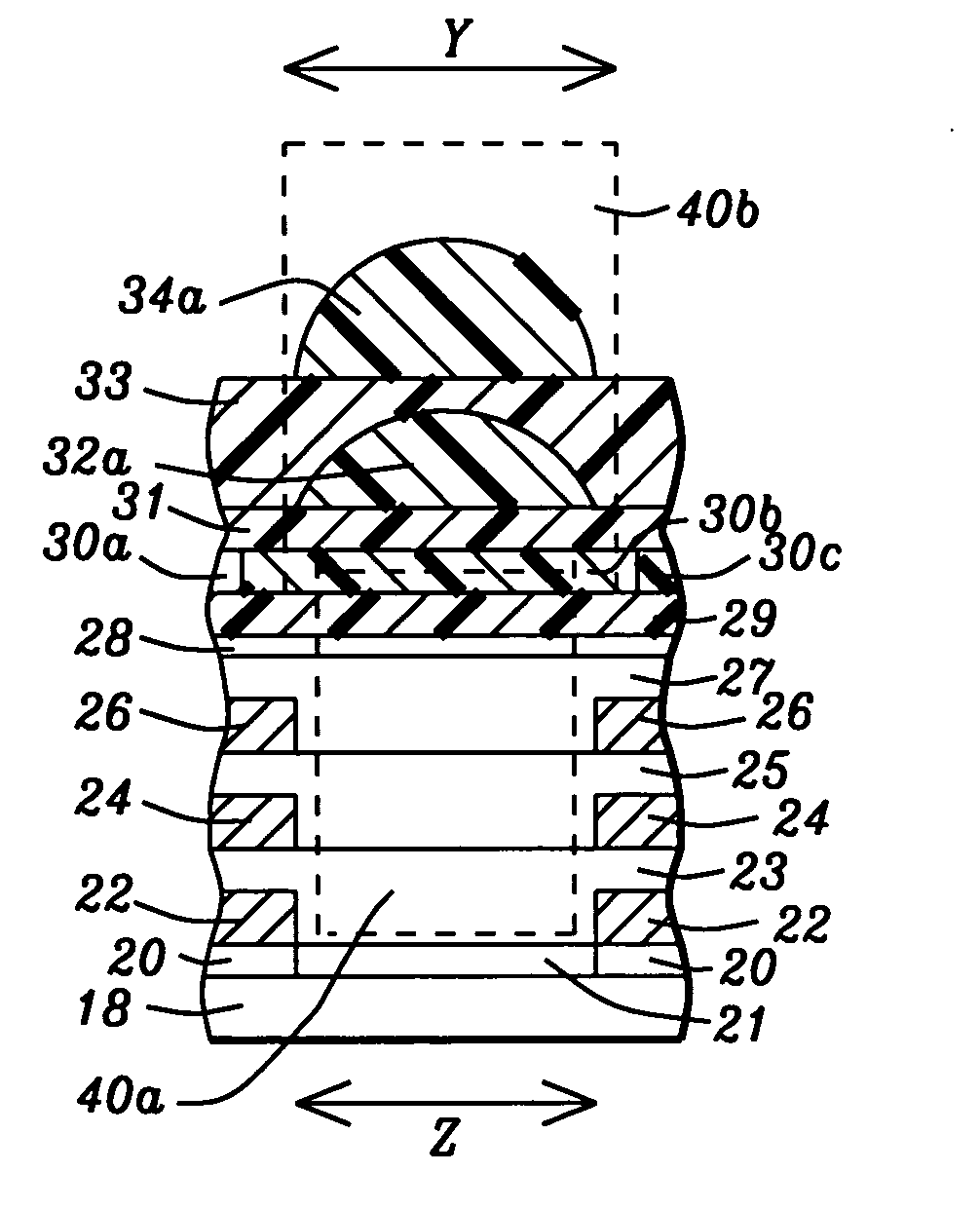
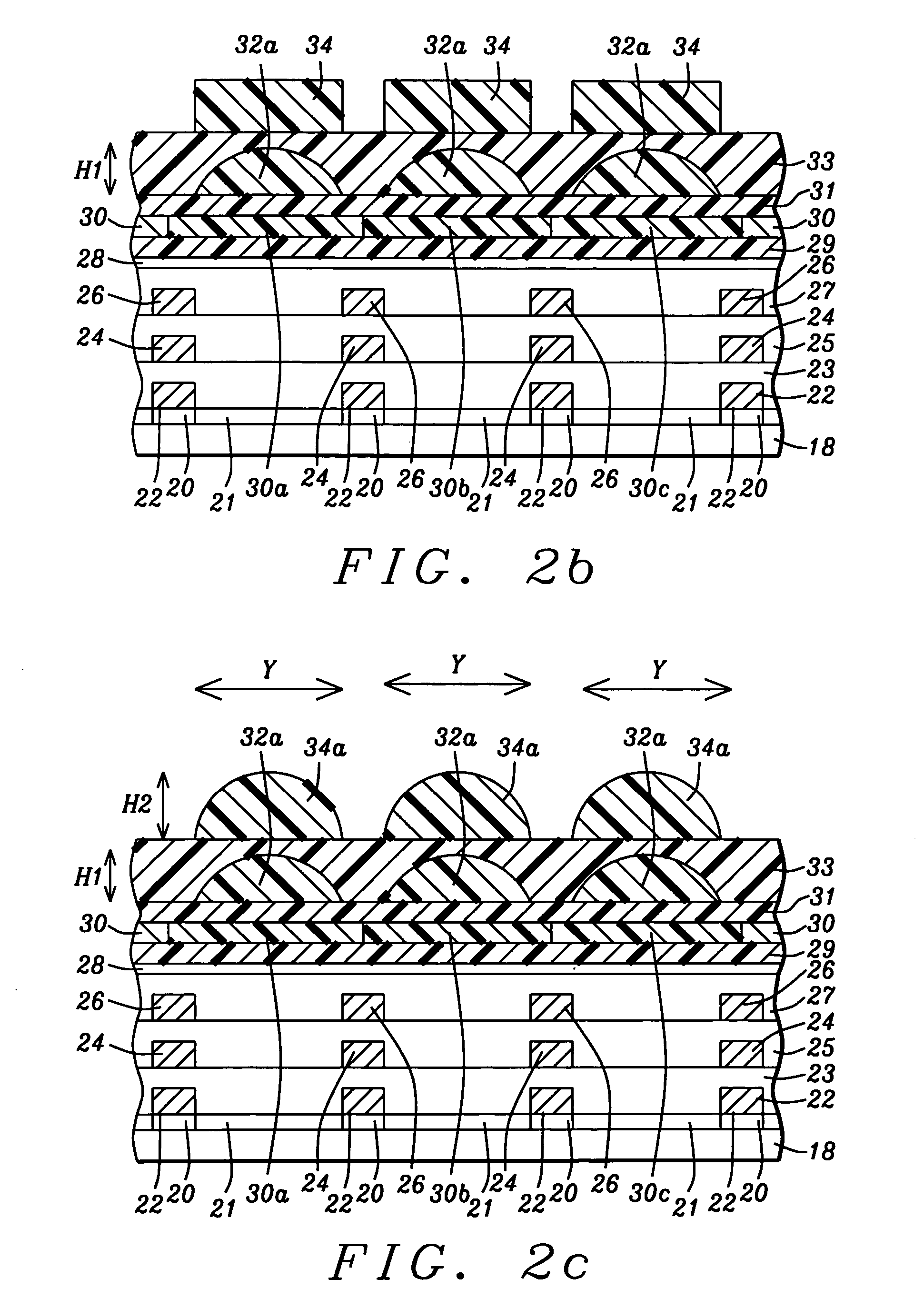
[0022] Referring to FIG. 2a, a substrate 18 is provided that may contain active and passive devices that are not shown in order to simplify the drawing. A lower stack of layers for a CMOS image sensor will now be described. A first dielectric layer 20 such as SiO2 is deposited on the substrate 18 and a photodiode array comprised of photodiodes 21 is fabricated within the first dielectric layer by conventional means. An interconnect structure comprised of a first metal (ILM) layer 22 is formed on dielectric layer 20 but not o...


PUM


Abstract

An image sensor device and method for forming said device are described. The image sensor structure comprises a substrate with photodiodes, an interconnect structure formed on the substrate, a color filter layer above the interconnect structure, a first microlens array, an overcoat layer, and a second microlens array. A key feature is that a second microlens has a larger radius of curvature than a first microlens. Additionally, each first microlens and second microlens is a flat convex lens. Thus, a thicker second microlens with a short focal length is aligned above a thinner first microlens having a long focal length. A light column that includes a first microlens, a second microlens and a color filter region is formed above each photodiode. A second embodiment involves replacing a second microlens in each light column with a plurality of smaller second microlenses that focus light onto a first microlens.

Description

FIELD OF THE INVENTION [0001] The invention relates to a solid state imaging device (hereafter referred to as a CMOS image sensor) and a method of manufacturing the same. More particularly, the image sensor has an improved microlens component that increases the sensitivity of the device. BACKGROUND OF THE INVENTION [0002] A complementary metal oxide semiconductor (CMOS) image sensor is a key component of many digital video cameras. The CMOS image sensor is typically comprised of an upper stack that includes one or more layers of color filters, a microlens array, and an overcoat for the microlens and a lower stack that includes interlevel dielectric (ILD) layers, interlevel metal (ILM) layers, and passivation layers which are fabricated on a substrate. High sensitivity is an important characteristic for a CMOS image sensor since the image quality may suffer if sensitivity is not high enough. The function of the microlens component is to focus light through a color filter layer and th...

Claims


Application Information

Patent Timeline
Patent Type & Authority Applications(United States)
IPC IPC(8): H01L27/00H01L27/146H01L31/00H01L31/0216H01L31/0232
CPCH01L27/14621H01L27/14623H01L27/14685H01L27/14627H01L27/14625
Inventor WENG, FU-TIENHSIAO, YU-KUNGCHANG, CHIN-KUNGHSU, HUNG-JENDAI, YI-MINGKUO, CHIN-CHEN
Owner TAIWAN SEMICON MFG CO LTD
Why Eureka
Try Eureka