Error recovery within processing stages of an integrated circuit

a technology of error recovery and integrated circuit, which is applied in the field of integrated circuits, can solve the problems of requiring a large number of delay latches to be added to the integrated circuit to implement error detection and recovery, and affecting the forward-progress of computation, etc., and achieves the effect of increasing the probability of errors in operation and reducing the likelihood of errors in operation

Active Publication Date: 2005-11-03
ARM LTD +1
View PDF57 Cites 96 Cited by
  • Summary
  • Abstract
  • Description
  • Claims
  • Application Information

AI Technical Summary

Benefits of technology

[0015] The stored recoverable state comprises at least a subset of architectural state variables corresponding to a programmers model of the integrated circuit. Using the stored recoverable state the error detection can be performed without the requirement to capture a delayed value from each processing stage or the requirement to reload the correct values into the processing logic in the event of an error in operation. This enables integrated circuits to be relatively easily modified so that the error detection and recovery can be applied to any critical path within the integrated circuit including both CPU data paths and control logic.
[0028] It will be appreciated that the operational parameter controller could be operable to adjust the performance controlling parameters in response to detection of an error in operation of the integrated circuit. The parameter adjustment could be performed immediately in response to detection of an error. For example the operating frequency could be reduced or the operating voltage increased to ensure that the likelihood of errors in operation is decreased. These adjustments could be perfromed at least temporarily. However, in one embodiment of the invention the response of adjusting the operational parameters by the operational parameter controller is damped so that the there is a time delay following detection of at least one error in operation before the adjustment of one or more of the performance controlling parameters. This allows the integrated circuit to assess the likelihood of the increased error rate persisting since such an increase may not be systematic and could be dealt with without adjustment of the operational parameters by simply re-executing the relevant sequence of processing operations. However, temporary adjustment of one or more operational parameters may be performed to prevent deadlock.

Problems solved by technology

Both the situation where the voltage level is reduced to the point at which the slowest processing stage can no longer keep pace and the situation where the operating frequency is increased to the point at which the slowest processing stage can no longer perform its processing will give rise to the occurrence of processing errors that will adversely effect the forward-progress of the computation.
However, the requirement to modify the processing circuit by providing a delayed latch for each main latch of the processing stages can in certain circumstances be inflexible.
For example, if operational errors are not restricted to the datapath of the central processing unit (CPU), but also occur in the control logic itself or in other critical paths of the integrated circuits then a considerable number of delay latches would have to be added to the integrated circuit to implement the error detection and recovery.
Furthermore, in embodiments of US-2004-0199821 that use existing pipeline sequencing logic to implement error recovery by reading data values from the delayed latches it may be difficult to ensure that the pipeline sequencing logic itself is not affected by errors in operation, either directly due to a critical path in the control logic itself or indirectly by feeding back a metastable value from the datapath into the control logic.

Method used


Image

  • Error recovery within processing stages of an integrated circuit
  • Error recovery within processing stages of an integrated circuit
  • Error recovery within processing stages of an integrated circuit

Examples


Embodiment Construction

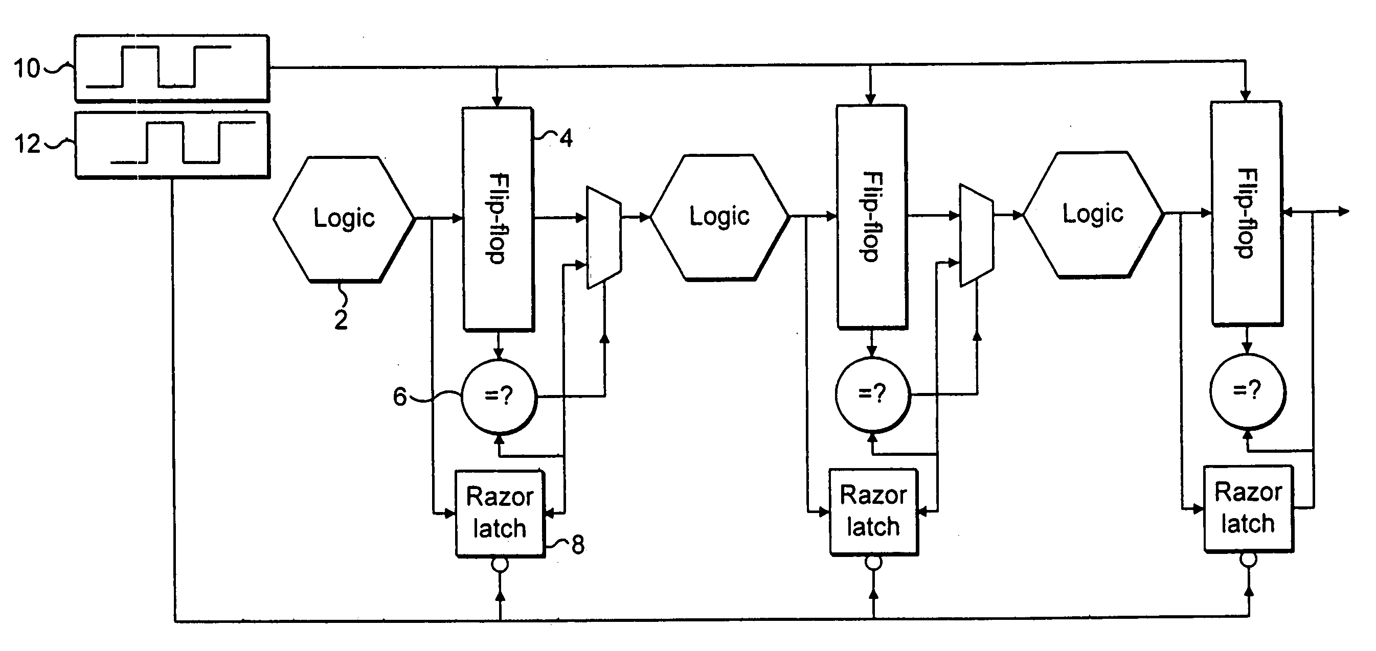
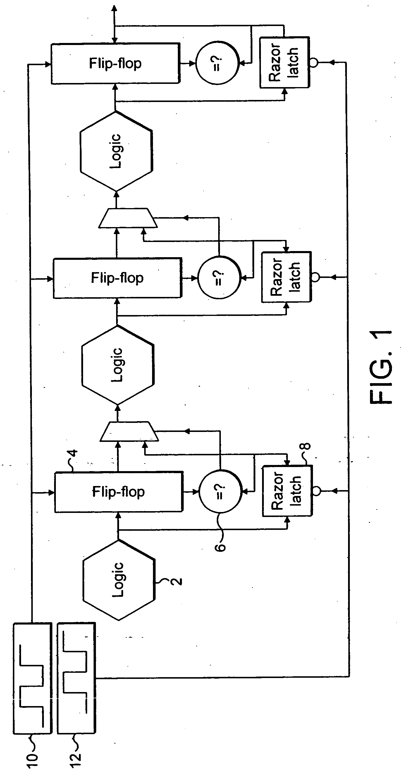
[0066]FIG. 1 illustrates a part of an integrated circuit, which may be a part of a synchronous pipeline within a processor core, such as an ARM processor core produced by ARM limited of Cambridge, England. The synchronous pipeline is formed of a plurality of like processing stages. The first stage comprises processing logic 2 followed by a non-delayed latch 4 in the form of a flip-flop together with a comparator 6 and a delayed latch 8. The term latch used herein encompasses any circuit element operable to store a signal value irrespective of triggering, clock and other requirements. Subsequent processing stages are similarly formed. A non-delayed clock signal 10 drives the processing logic and non-delayed latches 4 within all of the processing stages to operate synchronously as part of a synchronous pipeline. A delayed clock signal 12 is supplied to the delayed latches 8 of the respective processing stages. The delayed clock signal 12 is a phase shifted version of the non-delayed c...


PUM


Abstract

An integrated circuit includes a plurality of processing stages each including processing logic 1014 , a non-delayed signal-capture element 1016 , a delayed signal-capture element 1018 and a comparator 1024 . The non-delayed signal-capture element 1016 captures an output from the processing logic 1014 at a non-delayed capture time. At a later delayed capture time, the delayed signal-capture element 1018 also captures a value from the processing logic 1014 . An error detection circuit 1026 and error correction circuit 1028 detect and correct random errors in the delayed value and supplies an error-checked delayed value to the comparator 1024 . The comparator 1024 compares the error-checked delayed value and the non-delayed value and if they are not equal this indicates that the non-delayed value was captured too soon and should be replaced by the error-checked delayed value. The non-delayed value is passed to the subsequent processing stage immediately following its capture and accordingly error recovery mechanisms are used to suppress the erroneous processing which has occurred by the subsequent processing stages, such as gating the clock and allowing the correct signal values to propagate through the subsequent processing logic before restarting the clock. The operating parameters of the integrated circuit, such as the clock frequency, the operating voltage, the body biased voltage, temperature and the like are adjusted so as to maintain a finite non-zero error rate in a manner that increases overall performance.

Description

BACKGROUND OF THE INVENTION [0001] 1. Field of the Invention [0002] This invention relates to the field of integrated circuits. More particularly, this invention relates to the detection of operational errors within the processing stages of an integrated circuit and recovery from such errors. [0003] 2. Description of the Prior Art [0004] It is known to provide integrated circuits formed of serially connected processing stages, for example a pipelined circuit. Each processing stage comprises processing logic and a latch for storing an output value from one stage which is subsequently supplied as input to the succeeding processing stage. The time taken for the processing logic to complete its processing operation determines the speed at which the integrated circuit may operate. The fastest rate at which the processing logic can operate is constrained by the slowest of the processing logic stages. In order to process data as rapidly as possible, the processing stages of the circuit wil...

Claims


Application Information

Patent Timeline
Patent Type & Authority Applications(United States)
IPC IPC(8): G06F11/10G06F11/16
CPCG06F9/3861G06F9/3869G06F11/104G06F11/1608G06F11/0793G06F11/1695G06F11/183G06F11/0721G06F11/167
Inventor BLAAUW, DAVID THEODOREBULL, DAVID MICHAELDAS, SHIDHARTHA
Owner ARM LTD
Why Eureka
Try Eureka