
High voltage ESD-protection structure

a protection structure and high voltage technology, applied in the direction of semiconductor devices, semiconductor/solid-state device details, electrical apparatus, etc., can solve the problems of extremely thin dielectrics, high current clamping, and high voltage electrostatic discharge of semiconductor integrated circuit inputs and outputs, etc., to achieve enhanced high voltage esd clamping, reduce the size of an esd structure, and reduce the effect of current clamping

Active Publication Date: 2005-11-10
MICROCHIP TECH INC
View PDF15 Cites 4 Cited by
  • Summary
  • Abstract
  • Description
  • Claims
  • Application Information

AI Technical Summary

Benefits of technology

[0006] The invention overcomes the above-identified problems as well as other shortcomings and deficiencies of existing technologies by providing a high voltage ESD-protection structure that is effective is protecting sensitive input and / or output circuits from an ESD event by having a controlled breakdown at a voltage that is less than a voltage that may cause destructive breakdown of the input and / or output circuits, has enough current handling capabilities during the ESD event and does not snapback from the ESD event occurrence.
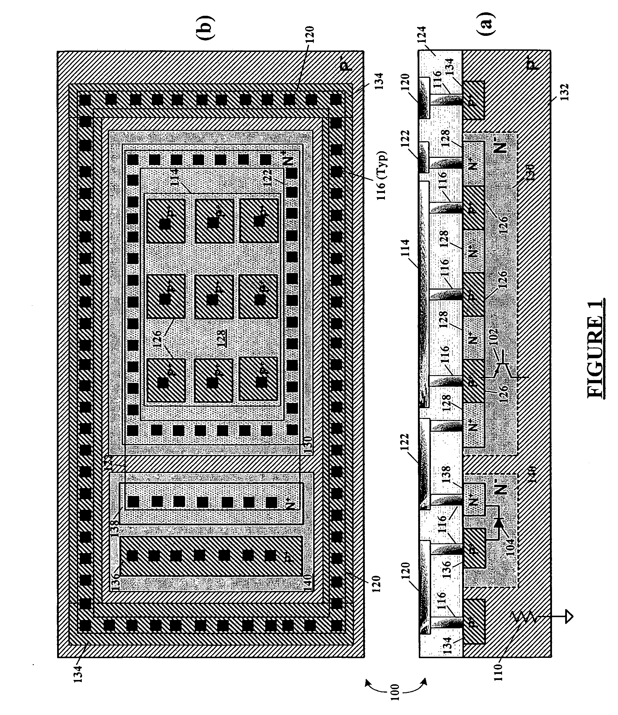
[0007] According to an embodiment of the invention, a high voltage ESD-protection structure may advantageously be located substantially under an integrated circuit bond pad. The high voltage ESD-protection structure protects the delicate transistor circuits connected to the bond pad from destructive high voltage ESD events by having a controlled breakdown at a voltage that is less than a voltage that may cause destructive breakdown of the input and / or output circuits. The high voltage ESD-protection structure is able to absorb high current from these ESD events without snapback that would compromise operation of the higher voltage inputs and / or outputs of the integrated circuit. The ESD-protection structure will conduct whenever an ESD event occurs at a voltage above a controlled breakdown voltage of an electronic device, e.g., diode, in the ESD-protection structure. Conduction of current from an ESD event having a voltage above the electronic device controlled breakdown voltage may be through another electronic device, e.g., transistor, having high current conduction capabilities, in the ESD-protection structure that may be controlled (triggered) by the device (e.g., diode) determining the controlled breakdown voltage (at which the ESD voltage is clamped to a desired value).
[0008] According to embodiments of the invention, a PNP transistor may be connected to an input and / or output pad of an integrated circuit device. The base of the PNP transistor may be connected to a diode having a controlled breakdown voltage having a desired trigger controlled breakdown voltage. When a voltage from an ESD event occurs that is greater than the controlled breakdown voltage of the electronic device, e.g., diode, the controlled breakdown voltage will cause the PNP transistor to conduct, e.g., from the input and / or output pad to ground. Since the PNP transistor structure is capable of conducting high transient currents, the PNP transistor structure will effectively and safely shunt any destructive voltage ESD event to ground. When the voltage at the ESD event voltage is below the controlled breakdown voltage, the PNP transistor will turn off and will not remain in a snapback condition, thus returning the input and / or output pad to full normal voltage operation.
[0009] According to embodiments of the invention, an ESD-protection structure may, but is not limited to, be located substantially under an integrated circuit bond pad in which further a low capacitance structure is formed by creating a forward diode between the bond pad and the ESD clamp circuit. Placing an ESD-protection structure under the bond pad may eliminate parasitic substrate capacitance. Furthermore a parasitic PNP transistor may be formed from the inserted forward biased diode.
[0014] A technical advantage is high current clamping of ESD transients. Another technical advantage is enhanced high voltage ESD clamping by the vertical PNP parasitic structure. Still another advantage is protection of higher voltage input and outputs of an integrate circuit. Yet another advantage is a non-snapback triggering of the ESD-protection clamping. Another technical advantage is reduce size for an ESD structure. Yet another technical advantage is isolating the bond pad from the substrate capacitance. Another technical advantage is reduced capacitance at a input or output node.

Problems solved by technology

The inputs and outputs of the semiconductor integrated circuits may be subject to undesirable high voltage electrostatic discharge (ESD) in addition to the desired input or output signal level.
An ESD event may create a sufficiently high voltage to cause destructive breakdown of transistor devices connected to the inputs and / or outputs of the semiconductor integrated circuits.
The extremely thin dielectric is very susceptible to damage by excessive voltages present in an ESD event that may cause destructive breakdown of an input and / or output device.
Attempts have been made to incorporate ESD protection within the integrated circuit, but are either not very effective, and / or require a significant amount of area within the integrated circuit die.
This is called “snapback” and is undesirable, especially when an input and / or output is adapted for high voltage operation (voltage being higher than a normal logic voltage level).
Use of the breakdown voltage of a diode for ESD protection has no snapback problems but lacked sufficient current handling for most ESD events.

Method used


Image

  • High voltage ESD-protection structure
  • High voltage ESD-protection structure
  • High voltage ESD-protection structure

Examples


Embodiment Construction

[0022] Referring now to the drawings, the details of exemplary embodiments of the present invention are schematically illustrated. Like elements in the drawing will be represented by like numbers, and similar elements will be represented by like numbers with a different lower case letter suffix. P− refers to lighter doped p-silicon, P+ refers to heavier doped p-silicon, N− refers to lighter doped n-silicon, and N+ refers to heavier doped n-silicon, wherein p-silicon has a plurality of positive immobile silicon ions, and n-silicon has a plurality of negative immobile silicon ions.

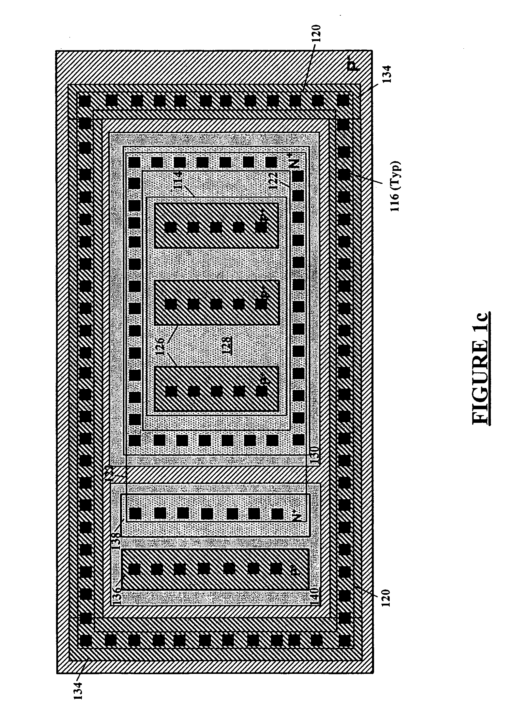
[0023] Referring to FIG. 1, depicted is a schematic diagram of a high voltage ESD-protection structure, according to an exemplary embodiment of the invention. FIG. 1a illustrates a sectional elevational view, FIG. 1b illustrates a plan view of the high voltage ESD-protection structure, and FIG. 1c illustrates a plan view of another high voltage ESD-protection structure. A semiconductor integrated circuit co...


PUM


Abstract

A high voltage ESD-protection structure is used to protect delicate transistor circuits connected to an input or output of an integrated circuit bond pad from destructive high voltage ESD events by conducting at a controlled breakdown voltage that is less than a voltage that may cause destructive breakdown of the input and / or output circuits. The ESD-protection structure is able to absorb high current from these ESD events without snapback that would compromise operation of the higher voltage inputs and / or outputs of the integrated circuit. The ESD-protection structure will conduct when an ESD event occurs at a voltage above a controlled breakdown voltage of an electronic device, e.g., diode, in the ESD protection structure. Conduction of current from an ESD event having a voltage above the electronic device controlled breakdown voltage may be through another electronic device, e.g., transistor, having high current conduction capabilities, in the ESD-protection structure that may be controlled (triggered) by the device (e.g., diode) determining the controlled breakdown voltage (at which the ESD voltage is clamped to a desired value). The high voltage ESD-protection structure may be located substantially under the bond pad and may also include a low capacitance forward diode structure between the bond pad and the ESD clamp circuit.

Description

FIELD OF THE INVENTION [0001] The present invention relates generally to semiconductor integrated circuits, and more particularly to protection of the semiconductor integrated circuits from electrostatic discharge (ESD). BACKGROUND OF THE INVENTION TECHNOLOGY [0002] Modern electronic equipment uses digital semiconductor integrated circuits for operation thereof. The digital semiconductor integrated circuits receive inputs from various sources, e.g., pushbuttons, sensors, etc., and have outputs that control operation of the equipment based upon the various inputs thereto. The inputs and outputs of the semiconductor integrated circuits may be subject to undesirable high voltage electrostatic discharge (ESD) in addition to the desired input or output signal level. The ESD, characterized by fast transient high voltage discharges, may be from static electricity generated by a user of the equipment, equipment handling, power supply voltage transients and the like. An ESD event may create ...

Claims


Application Information

Patent Timeline
Patent Type & Authority Applications(United States)
IPC IPC(8): H01L23/62H01L27/02
CPCH01L27/0259
Inventor YACH, RANDY L.DIX, GREGG
Owner MICROCHIP TECH INC
Learn More