Biosensor performance enhancement features and designs

a biosensor and performance enhancement technology, applied in the direction of diodes, radiation controlled devices, semiconductor devices, etc., can solve the problems of insufficient solution for biosensors, and insufficient solution for substrate reverse biases and biochemical attached charges, etc., to achieve the effect of improving biosensor performan

Inactive Publication Date: 2005-11-10
UNIV OF HAWAII
View PDF14 Cites 5 Cited by
  • Summary
  • Abstract
  • Description
  • Claims
  • Application Information

AI Technical Summary

Benefits of technology

[0009] The present invention may take several d

Problems solved by technology

Such leakage current, if blocking means are not provided, adds to the leakage current, creating a net increase in drain current and a drain voltage dependence of the drain current magnitude.
While one solution is to increase the field oxide thickness, and this is the solution typically used by industry (thick field oxide), this solution is insufficient for the biosensor for several reasons.
However, this solution will also fail for sufficient drain to substrate reverse biases and for some biochemical attached charge conditions.
This problem is non-obvious since n

Method used


Image

  • Biosensor performance enhancement features and designs
  • Biosensor performance enhancement features and designs
  • Biosensor performance enhancement features and designs

Examples


Embodiment Construction

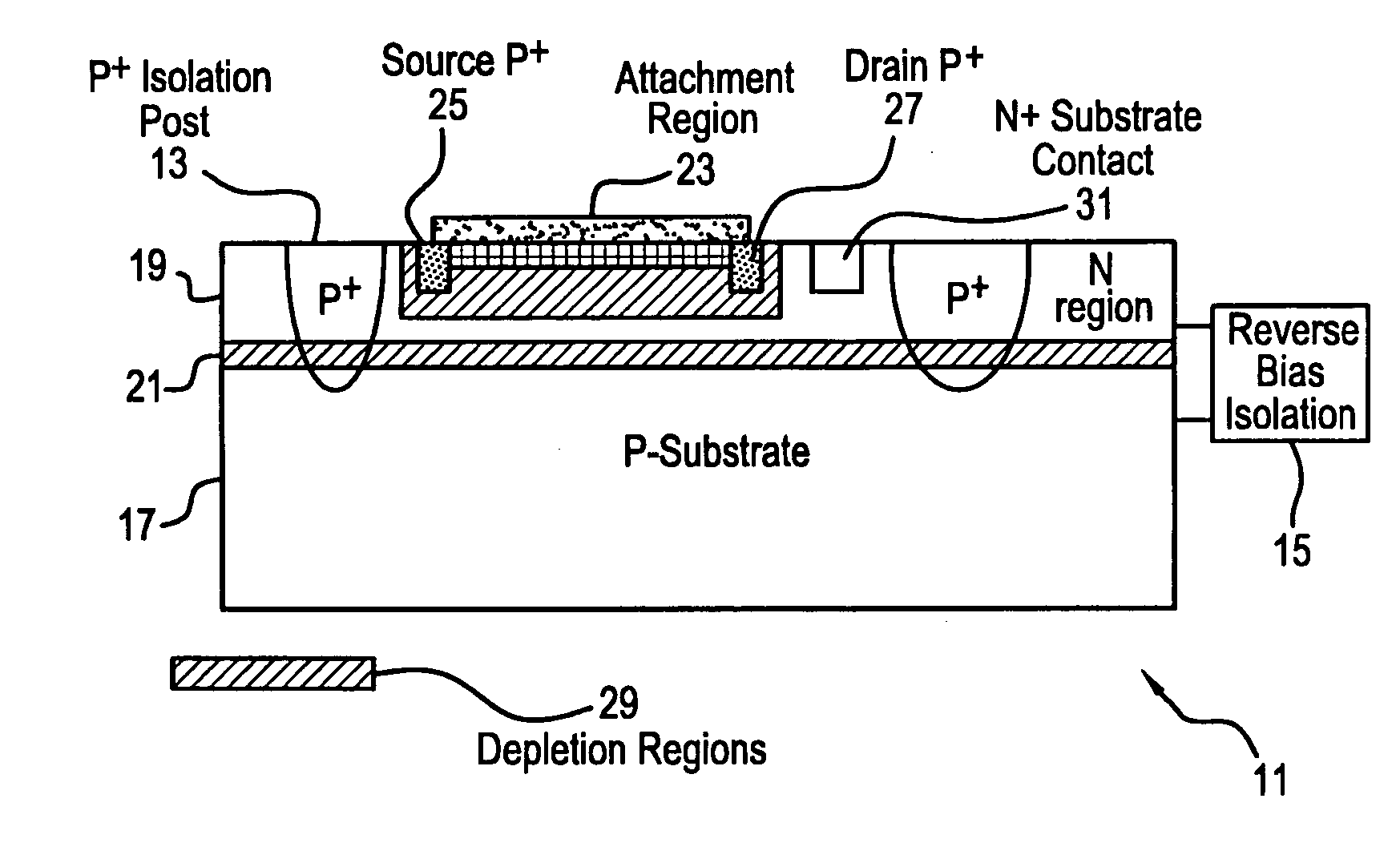
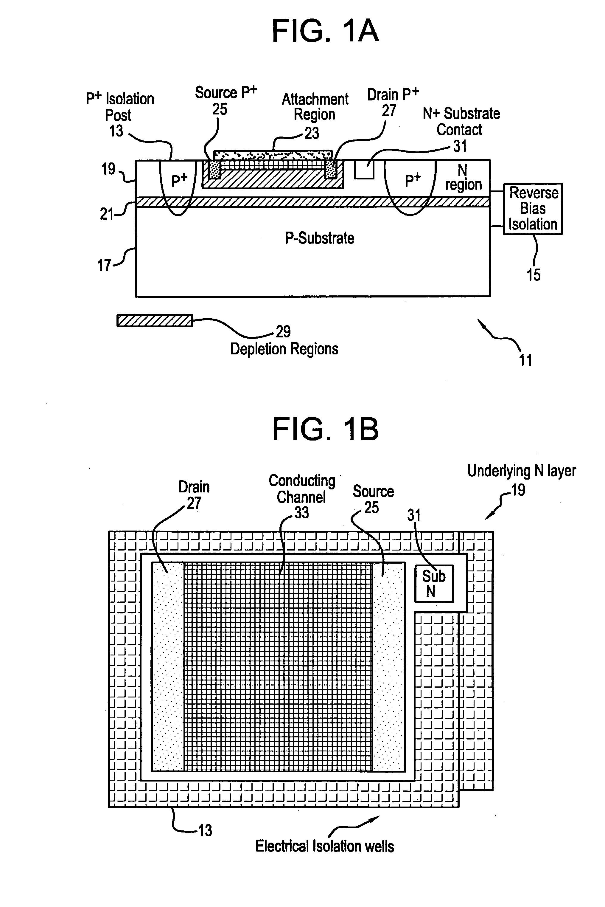
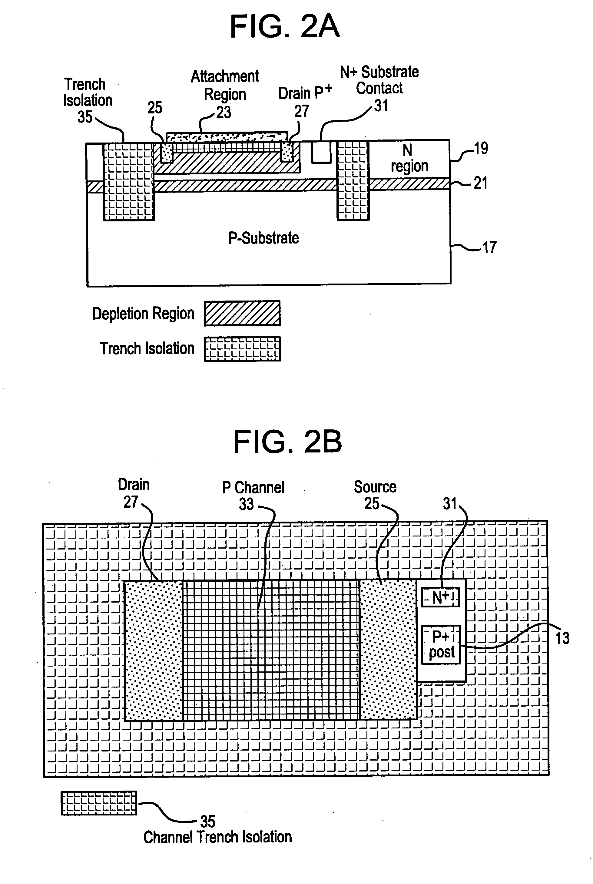
[0027] The present invention may take several different forms to improve biosensor performance. The first form is an increase in field oxide thickness. The field oxide is increased such that the difference between the substrate voltage and overlying drain and / or source conduit voltage creates an electric field across the field oxide that is lower than that needed to form an inversion layer and a pseudo PN junction.

[0028] Another form of improvement is to create P+ wells 13 to isolate the sensor from the substrate 17. An epitaxial N layer 19 is placed on a P substrate 17. A PN junction 21 provides basic isolation of the sensor from the substrate. However, by placing P+ posts 13 through the N epi layer 19, the N epi layer 19 is isolated from the remainder of the substrate. A back bias exists between the P region and the portion of the N-well containing the sensor, in this example, a P-Channel device. Here the well is made as small are possible depending on the size of the actual sens...


PUM


Abstract

Isolation of semiconductor based biosensors is described. The present invention is directed to prevention of undesirable influences including, but not limited to, chip leakage current. Several forms of sensor isolation and other protective means affect protection from adverse chip influences. The effect of biochemical attachment outside the sensor active region may have adverse effects on sensor performance. This potential problem is averted using protective design features.

Description

[0001] This application claims the benefit of U.S. Provisional Application No. 60 / 568,297, filed May 3, 2004, which is hereby incorporated by reference in its entirety.BACKGROUND OF THE INVENTION [0002] Electronic devices fabricated with integrated circuit (IC) technologies require biases and conduits to external contacts, where such biases are applied or measured and current is conducted into and out of the electronic devices. [0003] A conductor passing over an underlying substrate is isolated from the substrate by an oxide or insulator layer. The voltage of the interconnect line creates an electric field between the conducting interconnect line and the underlying substrate. If this electric field is sufficiently large, an accumulation or inversion layer may be formed. If an inversion layer forms, there is a depletion region separating the induced channel from the underlying semi-conducting substrate. If this junction is reverse biased, the underlying induced channel connects to th...

Claims


Application Information

Patent Timeline
IPC IPC(8): H01L21/336H01L21/8234H01L21/8238H01L27/146
CPCH01L27/14603H01L27/14643H01L27/1463H01L27/14609
Inventor HOLM-KENNEDY, JAMES W.
Owner UNIV OF HAWAII
Why Eureka
Try Eureka