Heterojunction far infrared photodetector

a far infrared and photodetector technology, applied in the field of photodetectors, can solve the problems of limitation, potential limit of hiwip use, etc., and achieve the effect of good ohmic contact and high doping

Inactive Publication Date: 2005-11-24
GEORGIA STATE UNIV RES FOUND INC
View PDF5 Cites 20 Cited by
  • Summary
  • Abstract
  • Description
  • Claims
  • Application Information

AI Technical Summary

Benefits of technology

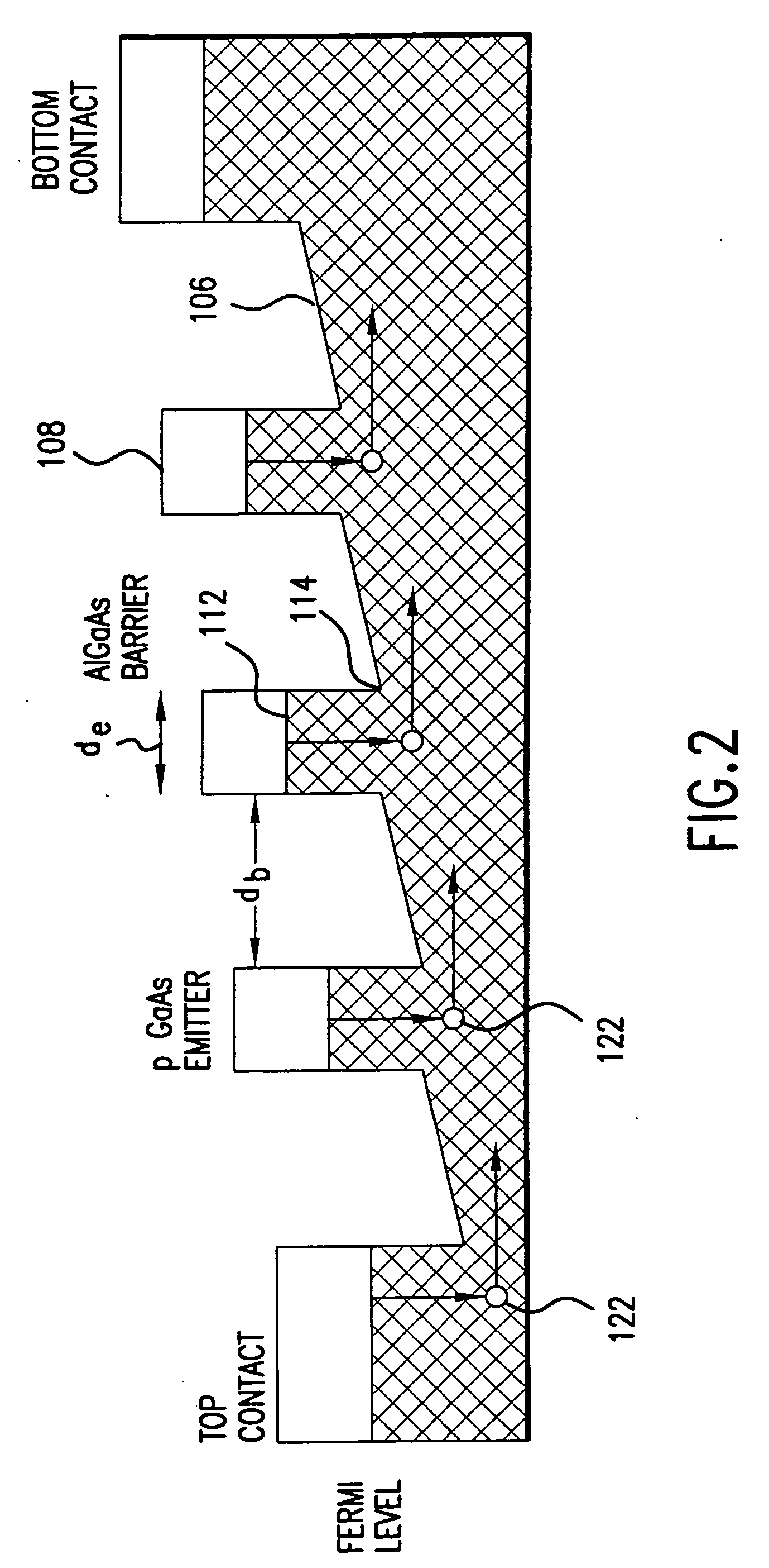
[0010] In one embodiment of the present invention, the third group III element is Ga, the first group II element is Be, and the second group V element is As. Other combinations of a group III element, a group II, IV or VI element and a group V element may be utilized to practice the present invention. The thickness of each emitter layer is at least 140 Å. For example, the thickness of each emitter layer is in the range of 140 to 200 Å. The doping concentration of Be is no more than 5×1018 cm−3. As an example, the doping concentration of Be is in the range of 1×1016 cm−3 to 5×1018 cm−3. The bandgap of each emitter is characterized by a workfunction substantially in the range of 20 to 22 meV for each heterojunction, wherein the workfunction of each emitter is the difference between the three dimensional Fermi level of the emitter and the conduction band of a corresponding barrier. Additionally, the total number of the emitters is no smaller than 5. For example, the total number of the emitters can be chosen as an integer in the range of 5 to 50.
[0011] At least one construction parameter of each barrier causes a sharp interface between any pair of neighboring emitter and barrier and a dark current at least 100 times less than that of a comparable HIWIP at a given temperature. Likewise, the construction parameters of each barrier are chosen from the group consisting of chemical identities of the first and second group III elements and the first group V element, thickness of the barrier layer, relative concentration of the first and second group III elements, the bandgap of the barriers, and the total number of the barriers.
[0012] In one embodiment of the present invention, the first group III element is Al, the second group III element is Ga, and the first group V element is As. Other combinations of two group III elements and a group V element may be utilized to practice the present invention. The concentration of the first group III element Al is characterized by a normalized amount x, x being in the range of 0 to 1, and the concentration of the second group III element Ga is characterized by a normalized relative amount 1-x. The thickness of each barrier layer is at least 600 Å. For example, the thickness of each barrier layer can be chosen in the range of 600 to 1000 Å. The total number of the barriers is no smaller than 6. For example, the total number of the barriers is an integer in the range of 6 to 51. The density of the dark current is somewhat inversely proportional to the total number of the barrier layers, N. In other words, the dark current is higher for a lower number of barriers but it is not a direct inverse proportionality. Moreover, the bandgap offset between the emitter and barrier materials is characterized by an activation energy in the range of 18 to 20 meV. For example, the bandgap offset is characterized by an activation energy substantially in the range of 18.5 to 19.5 meV. Note that in this embodiment, the thickness of each barrier layer is greater than the thickness of each emitter layer.
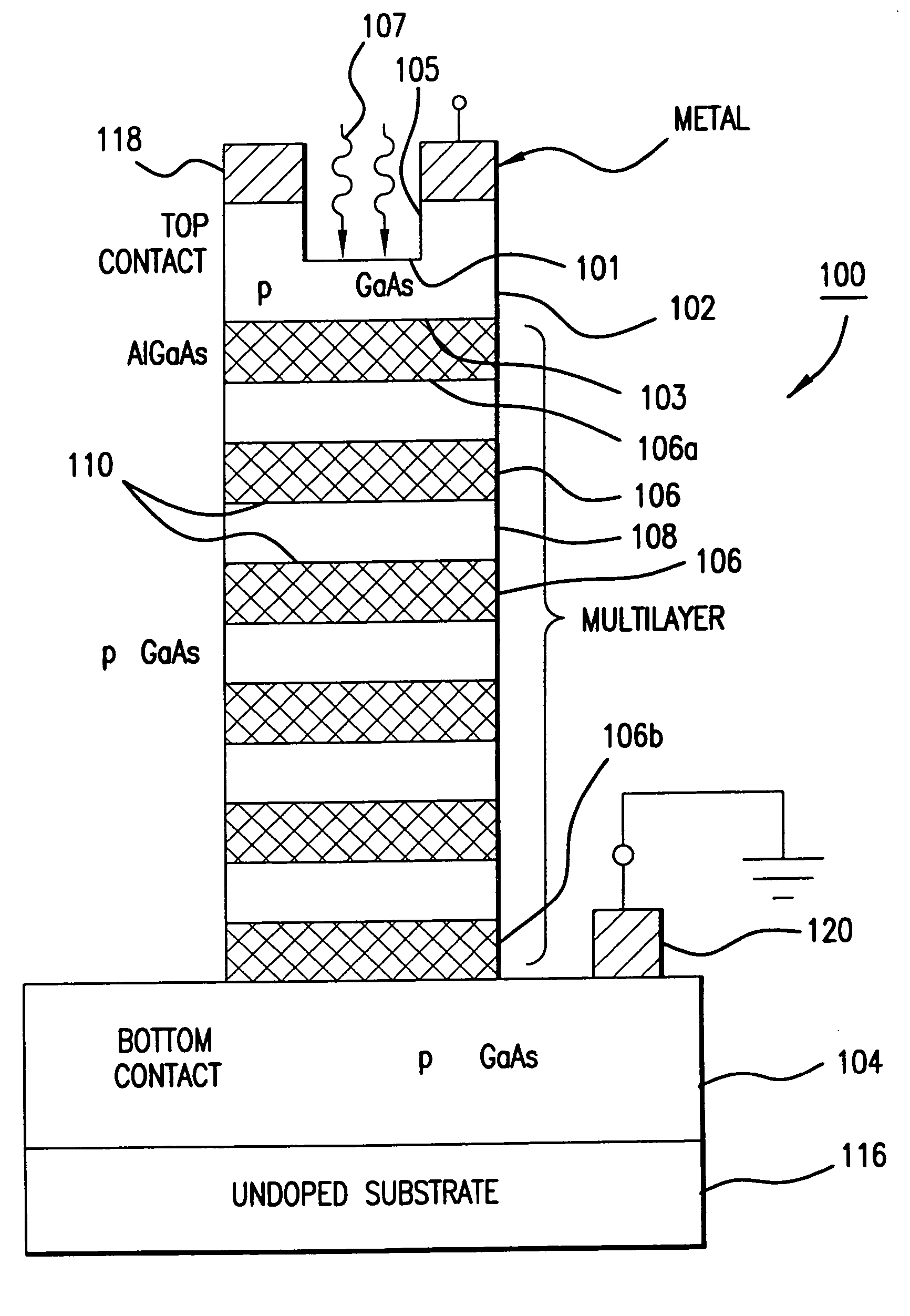
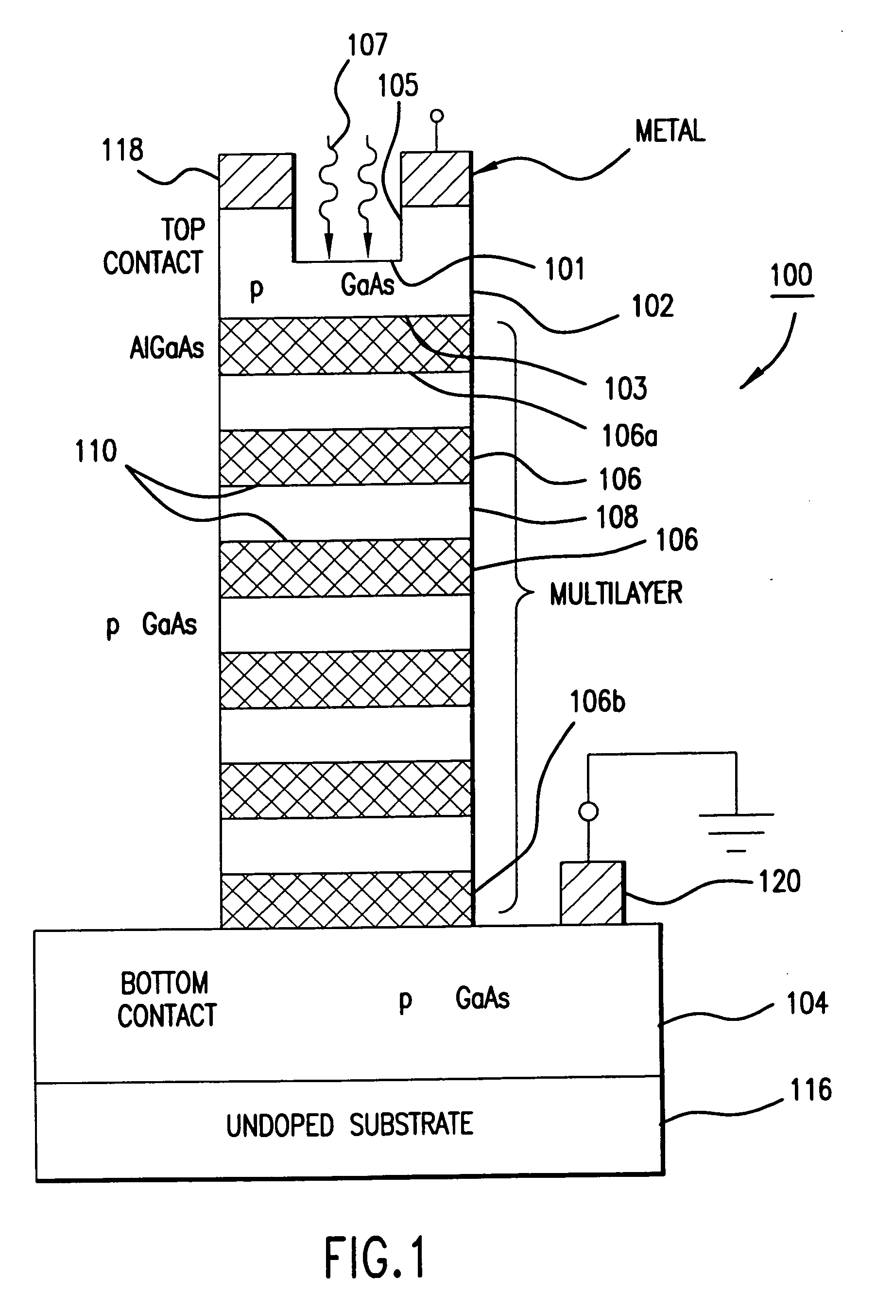
[0013] Furthermore, the photodetector has a first contact layer in contact with one outmost barrier, wherein the first contact layer is made from a material substantially identical to the material from which emitters are made. The first contact layer has a first surface and an opposite second surface, and an opening defined in the first surface to receive optical signals, the second surface being in contact with one outmost barrier. The first contact layer has a high doping in order to get a good ohmic contact. This material will absorb IR so some of the first contact may be removed. The photodetector also has a second contact layer opposite the first contact layer, wherein the second contact layer is made from a material substantially identical to the material from which emitters are made. The photodetector further has a substrate in contact with the second contact layer, wherein the first contact layer is made from a material substantially identical to the material from which emitters are made. Moreover, conductive contacts located at the first and second contact layers, respectively, can be utilized for measuring the response of the photodetector to the optical signals.
[0014] In another aspect, the present invention provides a photodetector. In one embodiment of the present invention, the photodetector has a plurality of N barriers, N being an integer greater than 1, each barrier being a layer of a material made from a first and a second group III elements and a first group V element and characterized by a bandgap. The photodetector also has a plurality of N−1 emitters, each emitter being a layer of material made from a third group III element and a second group V element and characterized by a bandgap different from that of the barriers and having at least one free carrier responsive to optical signals, wherein each emitter is located between two barriers so as to form a heterojunction at each interface between an emitter and a barrier. Moreover, each emitter is doped with a first group II, IV or VI element to cause free carriers in the emitter. At least one construction parameter of each barrier causes a sharp interface between any pair of neighboring emitter and barrier and a dark current at least 100 times less than that of a comparable HIWIP at a given temperature.

Problems solved by technology

HIWIP detectors have shown high responsivity and good detectivity in this range, but have their limitations.
However, even with the reduced diffusion, the high precision in doping density, and the uncertainty associated with the bandgap narrowing still place potential limits on the use of HIWIPs.
Another issue might be the direct transitions in the p-type (heavy hole and light hole) which is favored over indirect transitions.

Method used


Image

  • Heterojunction far infrared photodetector
  • Heterojunction far infrared photodetector
  • Heterojunction far infrared photodetector

Examples


Embodiment Construction

[0032] Several embodiments of the invention are now described in detail. Referring to the drawings, like numbers indicate like parts throughout the views. As used in the description herein and throughout the claims that follow, the meaning of “a,”“an,” and “the” includes plural reference unless the context clearly dictates otherwise. Also, as used in the description herein and throughout the claims that follow, the meaning of “in” includes “in” and “on” unless the context clearly dictates otherwise.

[0033] Additionally, as used in the description herein and throughout the claims that follow as known to people skilled in the art, a homojunction means a junction formed by two different electrical types of the same (band-gap) material. For example, a silicon p-n junction is a homojunction. A heterojunction means a junction formed by two different electrical types of two chemically different materials, each having a band-gap different from that of the other. An example of a heterojuncti...


PUM


Abstract

A photodetector and method of detecting far infrared optical signals. In one embodiment of the present invention, the photodetctor has a plurality of N barriers, N being an integer greater than 1, each barrier being a layer of a material made from a first and a second group III elements and a first group V element and characterized by a bandgap. The photodetector further has a plurality of N−1 emitters, each emitter being a layer of material made from a third group III element and a second group V element and characterized by a bandgap different from that of the barriers and having at least one free carrier responsive to optical signals, wherein each emitter is located between two barriers so as to form a heterojunction at each interface between an emitter and a barrier. Moreover, each emitter is doped with a first group II, IV or VI element to cause free carriers in the emitter, wherein at least one construction parameter of each emitter causes at least one free carrier to occupy a range of substantially continuously distributed energies characterized by a three dimensional Fermi level and respond to optical signals having wavelength in the range of 3 to 100 μm with significant absorption.

Description

CROSS-REFERENCE TO RELATED PATENT APPLICATION [0001] This application claims the benefit, pursuant to 35 U.S.C. § 119(e), of the provisional U.S. Patent Application Ser. No. 60 / 240,581 filed Oct. 16, 2000, entitled “Heterojunction Far Infrared Photodetector,” which application is hereby incorporated by reference in its entirety.BACKGROUND OF THE INVENTION [0002] 1. Field of the Invention [0003] The present invention generally relates to a photodetector. More particularly, the present invention relates to a far infrared photodetector utilizing a mechanism of detection based on free carrier absorption and internal photoemission over the bandgap offset of a heterojunction. [0004] 2. Description of the Related Art [0005] Far infrared (hereinafter “FIR”) detectors are of interest for various astronomy applications such as the Stratospheric Observatory For Infrared Astronomy (SOFIA) program and Explorer missions. Stressed Ge[1] (hereinafter “[n]” referring to the nth reference in the atta...

Claims


Application Information

Patent Timeline
Patent Type & Authority Applications(United States)
IPC IPC(8): H01L27/146H01L29/06H01L31/00H01L31/0304H01L31/0352H01L31/103H01L31/109
CPCB82Y20/00H01L27/14643H01L31/101Y02E10/544H01L31/03046
Inventor PERERA, A.G. UNILMATSIK, STEVEN GEORGE
Owner GEORGIA STATE UNIV RES FOUND INC
Why Eureka
Try Eureka