Quaternary and trinary logic switching circuits

Inactive Publication Date: 2005-11-24
CHANG AUGUSTINE W +1
View PDF10 Cites 11 Cited by
  • Summary
  • Abstract
  • Description
  • Claims
  • Application Information

AI Technical Summary

Benefits of technology

[0012] A logic circuit comprising a trinary or quaternary logic switching circuit which includes a multilevel storage cell (MLSC), and the variable threshold logic (VTL) means to yield an improved space, p

Problems solved by technology

However, conventional PCB subsystem assemblies still use standalone logic chips, memory chips, and discrete components interconnecting them with the PCB wiring.
However, typically the Flash transistor is not utilized as logic circuit element.
However, these devices are not utilized to make functional units by directly programming the threshold of the switch transistor and in configuring a basic logic circuit unit.
It is difficult to merge a Flash array with the CMOS-TTL logic circuit for the process and circuit compatibility issues, and there is no business advantage to merge these technologies for neither the manufacturers of FPGA nor the manufacturers of Memory standard parts.
However, many p

Method used


Image

  • Quaternary and trinary logic switching circuits
  • Quaternary and trinary logic switching circuits
  • Quaternary and trinary logic switching circuits

Examples


Embodiment Construction

[0028] The present invention relates generally to integrated circuits and more particularly to multileveled logic switching circuits. The following description is presented to enable one of ordinary skill in the art to make and use the invention and is provided in the context of a patent application and its requirements. Various modifications to the preferred embodiment and the generic principles and features described herein will be readily apparent to those skilled in the art. Thus, the present invention is not intended to be limited to the embodiment shown but is to be accorded the widest scope consistent with the principles and features described herein.

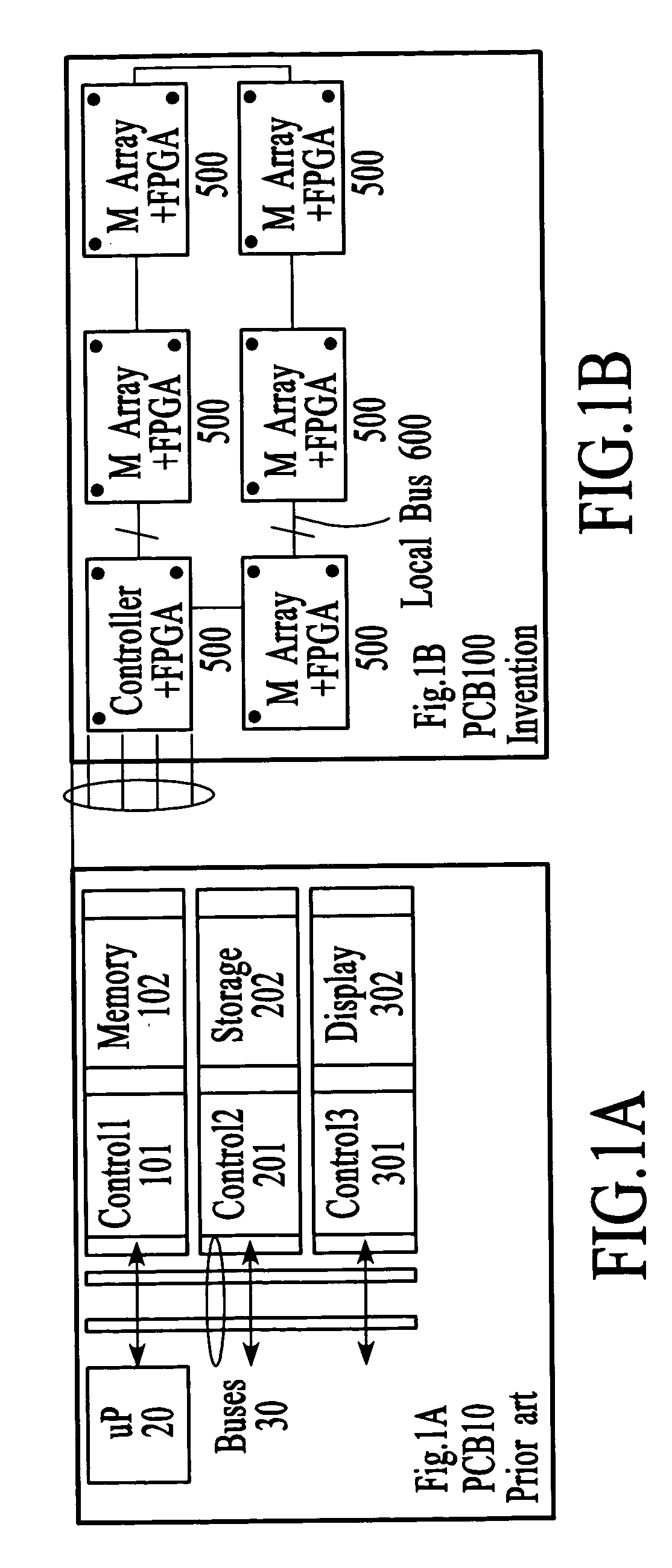
[0029] The present invention utilizes device and system architecture for providing intelligent nonvolatile subsystems. The nonvolatile subsystem encompasses embedded units of Flash and memory arrays (SRAM, DRAM, ROM) and programmable logic arrays. The goal is to optimize an organization of low cost, high capacity, distributive c...


PUM


Abstract

A logic circuit comprising a quaternary logic switching circuit which includes a multilevel storage cell (MLSC), and the trinary or variable threshold logic means to yield an improved space, power, and time-efficient performance device is disclosed. The present invention is used for the implementation of a customized new logic design to further improve the cost-effectiveness of the application. Advanced circuit solutions are provided using asynchronous clock controlled functional units which are field programmable. A diode capacitor ladder chain is also used on an on-chip power supply multiplier to support internal high voltage operations. A digital-to-analog-to-digital translation (DADT) apparatus is also provided utilizing the above identified circuits. Finally, a printed circuit board (PCB) net driver with a trinary signal wire provides 50% bandwidth increase over conventional binary solutions.

Description

RELATED APPLICATIONS [0001] The present invention is related to copending U.S. patent application entitled “3D Flash EEPROM Cell and the Methods of Implementing the Same”, Ser. No. 10 / 800,257, filed on Mar. 11, 2004, and assigned to the assignee of the present invention; and copending U.S. patent application entitled “Variable Threshold Transistor for the Schottky FPGA and Multilevel Storage Cell Flash Arrays”, Ser. No. 10 / 817,201, filed on Apr. 2, 2004, and assigned to the assignee of the present invention which is related to copending U.S. patent application entitled “SCL Type FPGA with Multi-Threshold Transistors and Method for Forming Same”, Ser. No. ______ (3070P) filed on Apr. 19, 2004, and assigned to the assignee of the present invention, and U.S. patent application entitled “Distributive Computing Subsystem of Generic IC Parts”, Ser. No. ______, (3072P) filed on May 7, 2004, and assigned to the assignee of the present invention, all of which are incorporated by reference he...

Claims


Application Information

Patent Timeline
IPC IPC(8): H01L27/105H03K3/038H03K19/00H03K19/02
CPCH01L27/105H03K19/0002H03K3/038
Inventor CHANG, AUGUSTINE W.KAO, I-PIENG PETER
Owner CHANG AUGUSTINE W
Why Eureka
Try Eureka