Surface acoustic wave device and communication apparatus
- Summary
- Abstract
- Description
- Claims
- Application Information
AI Technical Summary
Benefits of technology
Problems solved by technology
Method used
Image

Examples
examples
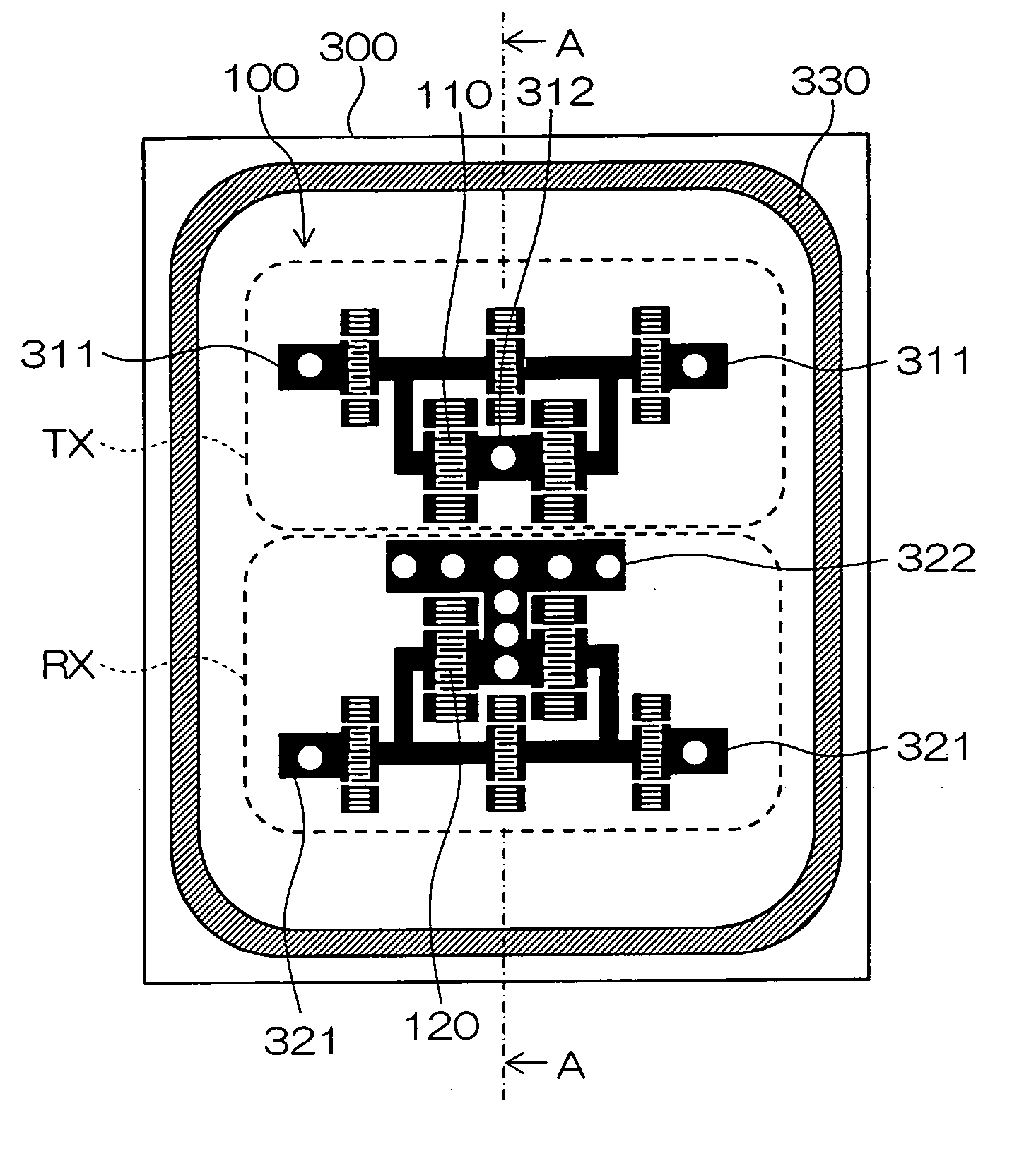
[0146] A surface acoustic wave device shown in FIGS. 7 and 8 was manufactured.
[0147] In a surface acoustic wave element, a 38.7-degree Y-cut X-propagation lithium tantalate single crystal substrate was used as a piezoelectric substrate, and IDT electrodes 110 and 120 composed of an Al alloy of Al (99% by mass) —Cu (1% by mass), ground electrodes 312 and 322, signal input / output electrodes 311 and 321, and a wiring electrode and a grounding annular electrode 330 for electrically connecting the electrodes were formed on its main surface.
[0148] The electrodes were produced by forming an Al alloy thin film using a sputtering method, then subjecting the thin film to photolithography using a spin-coater, a stepper, a developer, etc., etching the thin-film by the RIE (Reactive Ion Etching) apparatus, etc. to form predetermined patterns.
[0149] A circuit board was produced by laminating a plurality of insulating layers. Ceramics (a dielectric constant 9) mainly composed of alumina was use...
PUM
 Abstract
Description
Claims
Application Information