Semiconductor memory device and operating method of the same

a memory device and semiconductor technology, applied in the field of semiconductor memory devices and methods of operating the same, can solve the problems of pseudo sram suffering from the reduced access speed of the memory array, sram may dissatisfy a required specification, and the recent requirements of electronic devices, so as to improve the flexibility of burst write operation

Inactive Publication Date: 2005-12-01
RENESAS ELECTRONICS CORP
View PDF2 Cites 10 Cited by
  • Summary
  • Abstract
  • Description
  • Claims
  • Application Information

AI Technical Summary

Benefits of technology

[0015] The semiconductor memory device thus constructed allows the write operation to be aborted in the middle of the burst cycle. In response to the abortion of the write operation being requested, the write amplifier selectively writes the write data stored in the relevant write register into the memory array. The write operation thus described allows the semiconductor memory device to selectively write the desired write data stored in the write registers without a data mask signal. This effectively improves flexibility of burst write operation.

Problems solved by technology

The SRAM, however, often dissatisfies recent requirements of electronic devices due to the poor integration capability.
Recent high-end electronic devices require a work memory having an increased capacity, and an SRAM may dissatisfy a required specification as a work memory.
One drawback is that the pseudo SRAM suffers from the reduced access speed to the memory array, compared to the SRAM.
Therefore, the improvement of the access speed is one of the most important issues for using a pseudo SRAM as a work memory.
Conventional pseudo SRAMs, however, are not adapted to selective data transfer of write data from the write register to the memory cells; pseudo SRAMs are conventionally designed to concurrently transfer the complete set of the write data.
The selective data write technique based on the data mask signal, however, is not applicable to the pseudo SRAM, because the standard SRAM interface is not adapted to the data mask signal.

Method used


Image

  • Semiconductor memory device and operating method of the same
  • Semiconductor memory device and operating method of the same
  • Semiconductor memory device and operating method of the same

Examples


first embodiment

(Device Structure)

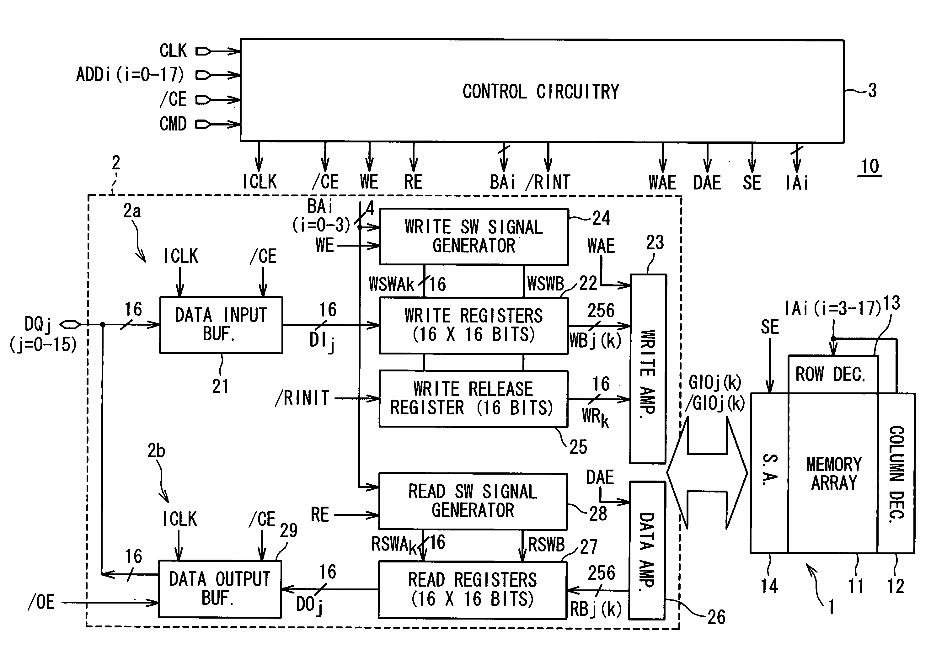
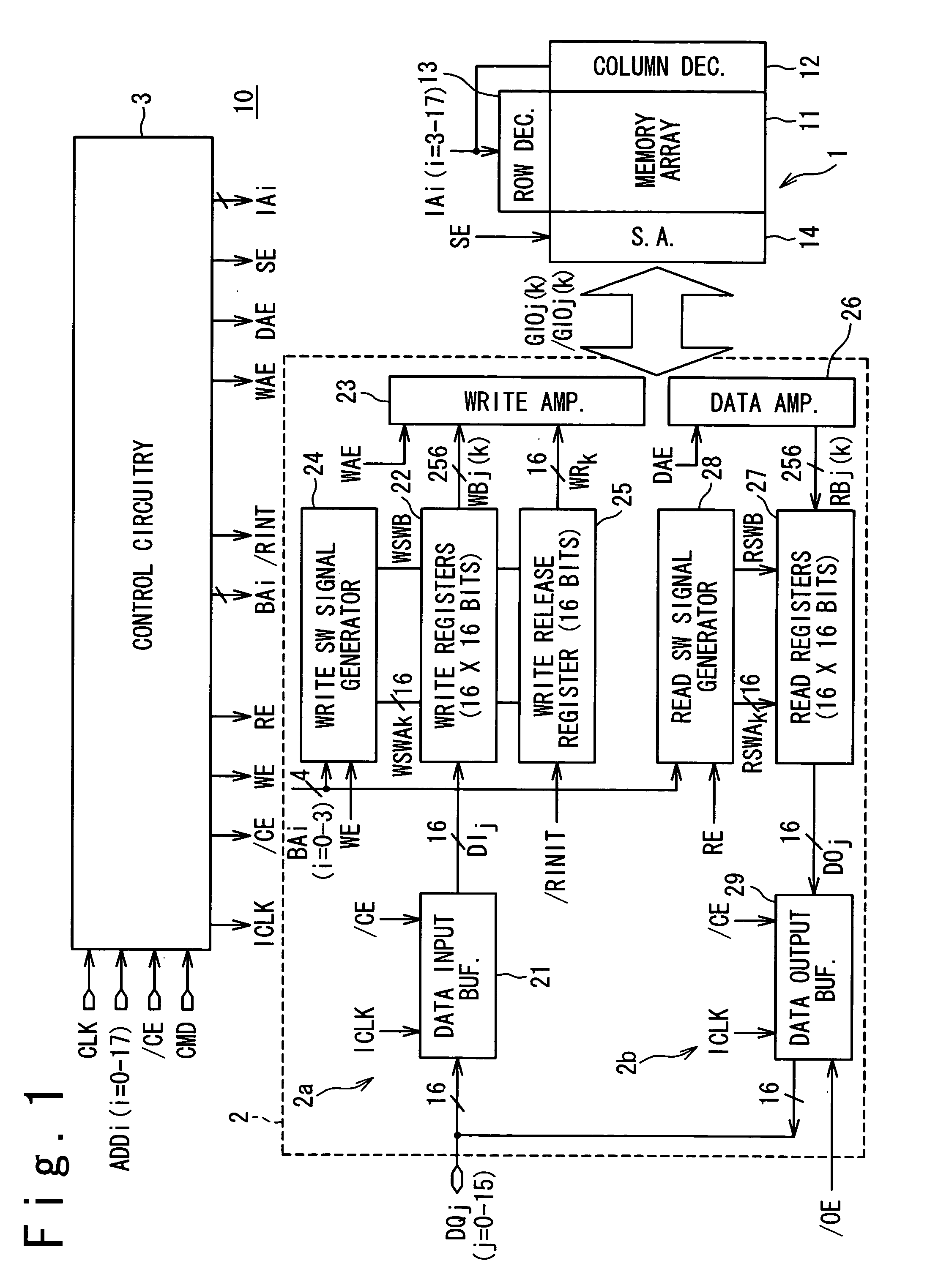
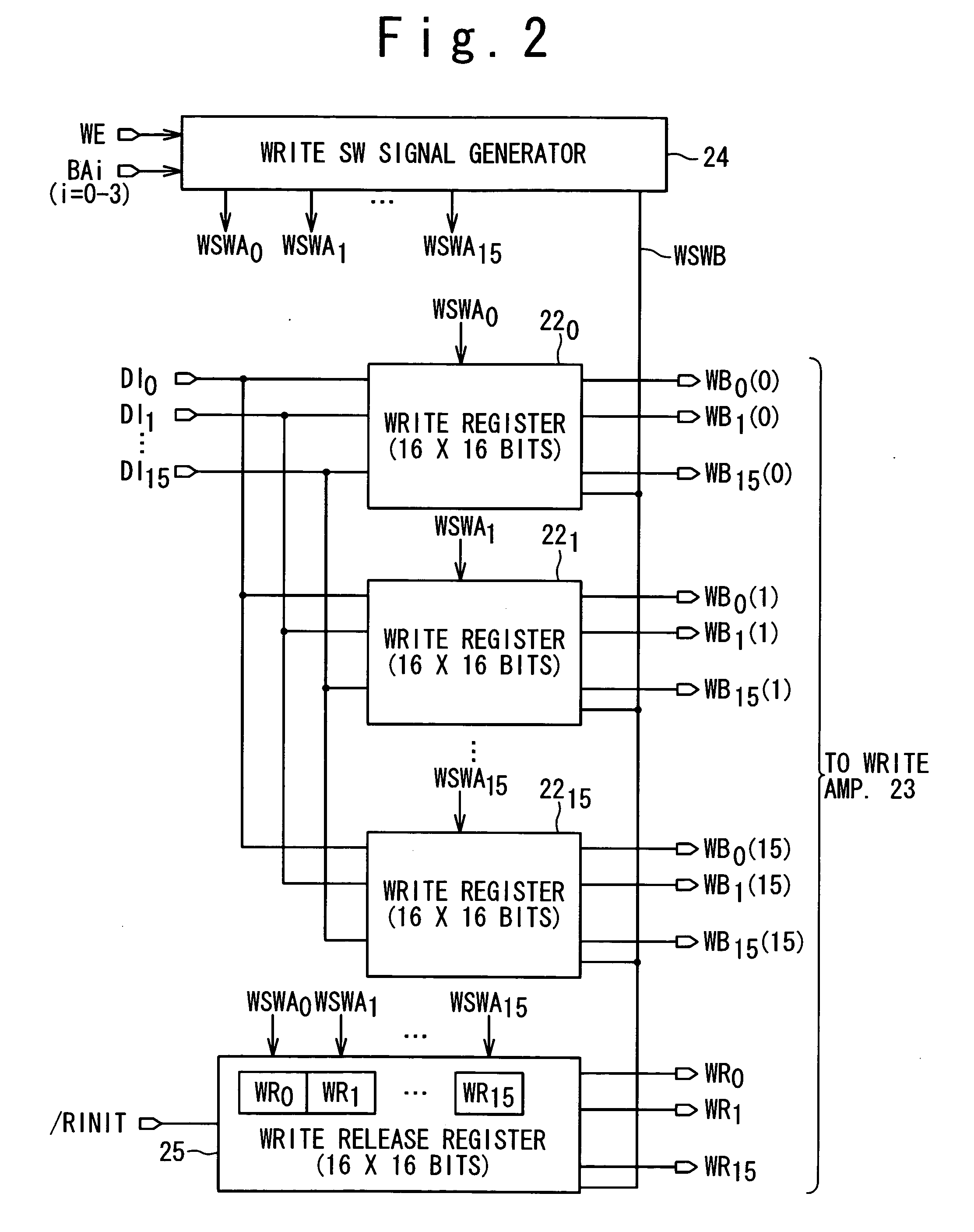
[0047] In a first embodiment, a pseudo SRAM 10 is provided with a memory circuitry 1, a data interface circuitry 2, and a control circuitry 3.

[0048] The memory circuitry 1 is composed of a memory array 11, a column decoder 12, a row decoder 13, and a sense amplifier circuit 14. The memory array 11 includes DRAM cells arrange in rows and columns (not shown). The column decoder 12, the row decoder 13 and the sense amplifier circuit 14 are used to provide access to a selected memory cell. Specifically, the column decoder 12 selects the column associated with the selected memory cell, and the row decoder 13 selects the row associated with the selected memory cell. The sense amplifier circuit 14 is used for identifying the data stored in the selected memory cell, and for writing desired data into the selected memory cell.

[0049] The data interface circuitry 2 provides access to the memory circuitry 1 based on burst transmission. The data interface circuitry 2 is conn...

second embodiment

(Device Structure)

[0103]FIG. 10 is a block diagram illustrating the structure of the pseudo SRAM 20 in a second embodiment. The structure of the pseudo SRAM 20 in the second embodiment is almost similar to that of the pseudo SRAM 10 shown in FIG. 1; the difference is that the pseudo SRAM 20 is designed to provide individual data access of upper and lower bytes for the memory array 11; the upper bytes designates the bytes associated with the data pins DQ8-DQ15, while the lower bytes designates the bytes associated with the data pins DQ0-DQ7. In order to achieve the individual data access of the upper and lower bytes, a set of byte select signals / UB and / LB are externally provided for the pseudo SRAM 20. The upper byte select signal / UB is used to enable the access of the upper bytes, while the lower byte select signal / LB is used to enable the access of the lower bytes. More specifically, the structure of the pseudo SRAM 20 is different from that of the pseudo SRAM 10 shown in FIG...


PUM


Abstract

A semiconductor memory device adapted to burst transmission is provided for improving flexibility of data write operation. The semiconductor memory device is composed of: a memory array; a set of write registers; an input buffer designed to sequentially receive a series of write data during a burst cycle, and to write said write data into associated ones of said write registers; a write release register containing a set of write release flags associated with said write registers, respectively; a write release register controller asserting associated ones of said write release flags in response to said write data being written into said associated ones of said write registers; and a write amplifier designed to concurrently write said write data contained in said write registers associated with asserted ones of said write release flags, selectively, when said burst cycle is aborted in response to a control signal.

Description

BACKGROUND OF THE INVENTION [0001] 1. Field of the Invention [0002] The present invention relates to semiconductor memory devices and method of operating the same, and more particularly, relates to semiconductor memory devices adapted to burst transmission. [0003] 2. Description of the Related Art [0004] The Static Random Access Memory (SRAM) is a typical semiconductor memory device used as a work memory for data processing. Using an SRAM as a working memory effectively achieves high speed data processing due to the enhanced operation speed. [0005] The SRAM, however, often dissatisfies recent requirements of electronic devices due to the poor integration capability. Recent high-end electronic devices require a work memory having an increased capacity, and an SRAM may dissatisfy a required specification as a work memory. This necessitates an alternative semiconductor memory with an increased capacity, suitable as a work memory. [0006] The pseudo SRAM is a semiconductor memory device ...

Claims


Application Information

Patent Timeline
Patent Type & Authority Applications(United States)
IPC IPC(8): G11C7/00G11C11/407G11C7/10G11C11/409
CPCG11C7/1006G11C7/1087G11C7/1078G11C7/1018
Inventor ISHIZAKI, TATSUYA
Owner RENESAS ELECTRONICS CORP
Why Eureka
Try Eureka