Wiring substrate and method of fabricating the same

a technology of wiring substrate and substrate, which is applied in the direction of printing element electric connection formation, transportation and packaging, chemistry apparatus and processes, etc., can solve the problems of poor adhesion between the film formed by electroless plating and the film formed by electroplating, and the reliability of wiring is less, so as to improve the reliability of wiring substrate

Inactive Publication Date: 2005-12-01
SANYO ELECTRIC CO LTD
View PDF11 Cites 12 Cited by
  • Summary
  • Abstract
  • Description
  • Claims
  • Application Information

AI Technical Summary

Benefits of technology

[0009] The present invention has been done in view of the aforementioned circumstances and its object is to provide a technique for improving the reliability of a wiring substrate in which a metal material is formed.

Problems solved by technology

One problem with forming a copper via in two stages as described above is that adhesion between the film formed by electroless plating and the film formed by electroplating is poor.
Another problem is that stress migration or electromigration occurs at an interface between the films, making the wiring less reliable.

Method used


Image

  • Wiring substrate and method of fabricating the same
  • Wiring substrate and method of fabricating the same
  • Wiring substrate and method of fabricating the same

Examples


example

Example 1

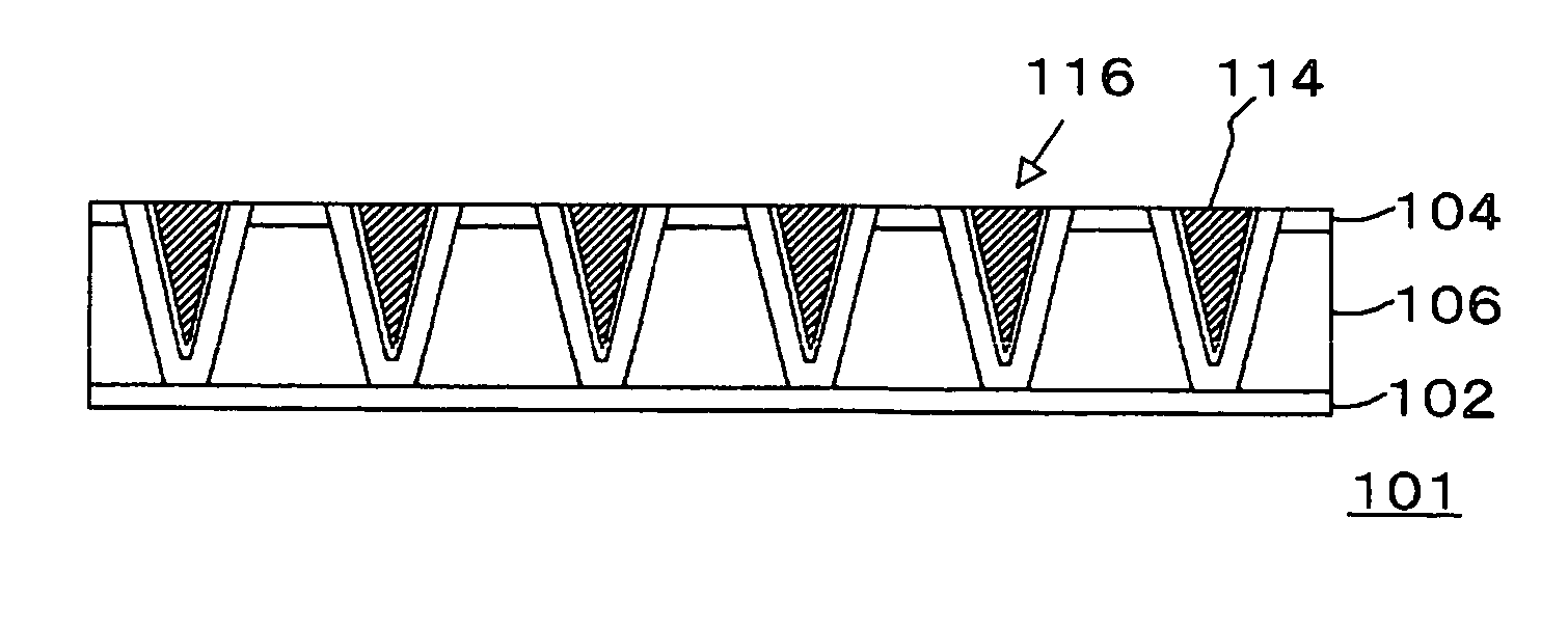
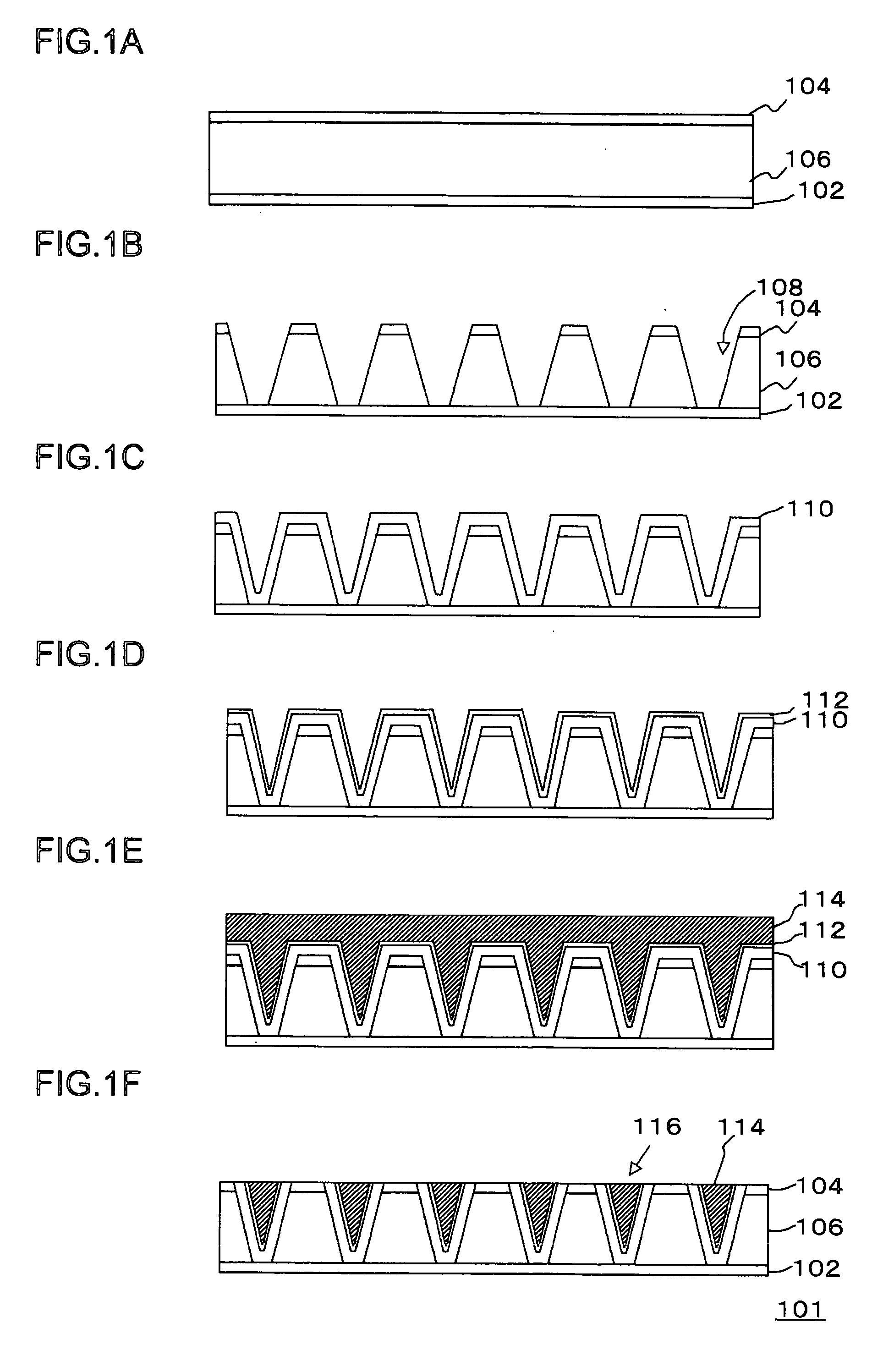
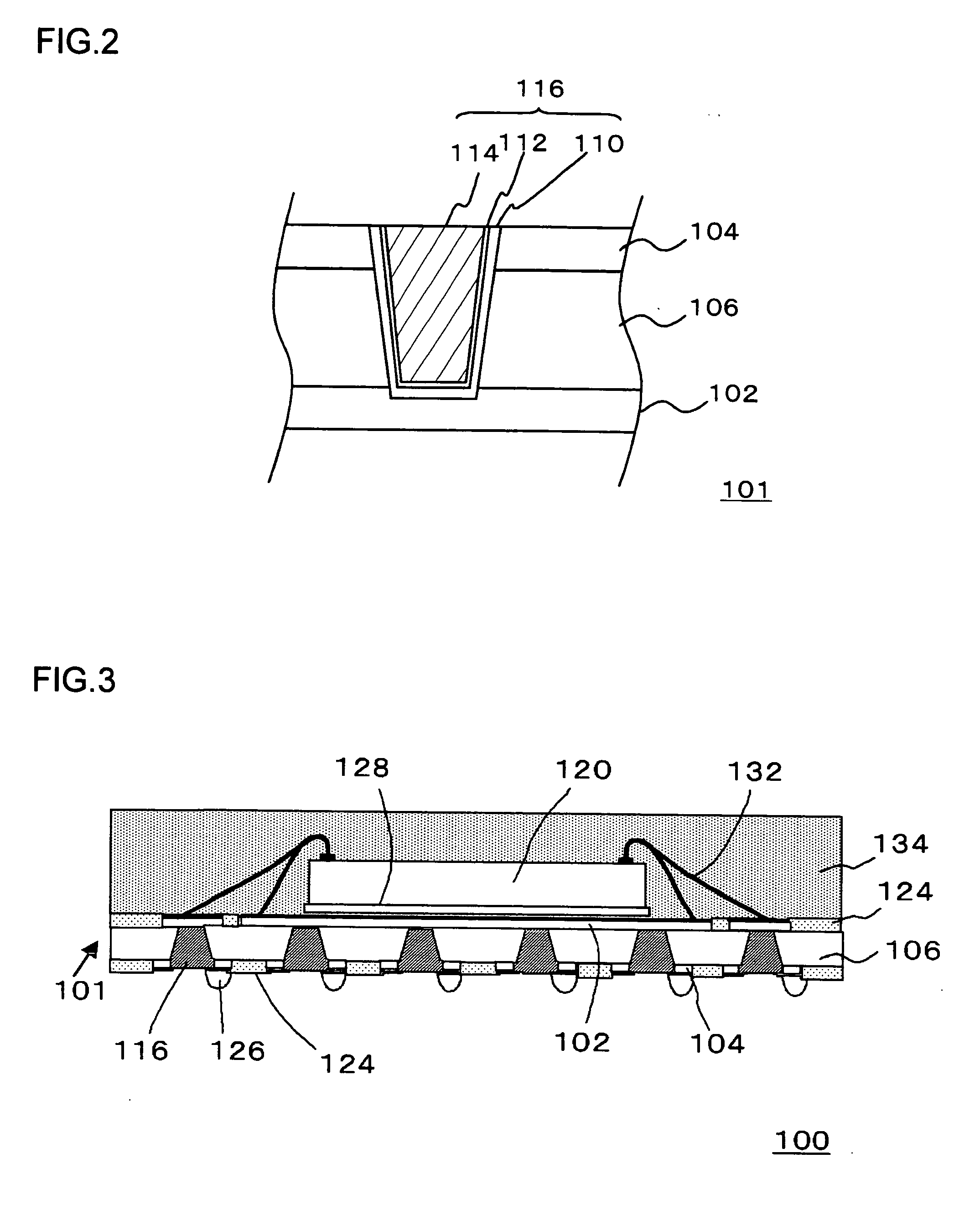
[0040] A via hole is formed as described in the above embodiment. The first metal film 110 (about 1 μm) is formed in the via hole by electroless plating. The metal oxide film 112 (about 1 nm) is formed by spraying the surface of the first metal film 110 with an oxygen gas at a high pressure (about 500 kPa). Further, the second metal film 114 (about 20 μm) is formed on the metal film 112 by electroless plating. With this, the via 116 is formed. FIG. 4 is a section illustrating the structure of the via thus formed.

[0041]FIG. 5 is a transmission electron micrograph showing a magnified view of an encircled part of FIG. 4. A granular low-contrast portion is observed in the micrograph. The low-contrast portion is considered to be an amorphous oxide film. This demonstrates that the metal oxide film 112 is formed between the first metal film 110 and the second metal film 114 by spraying of an oxidizing gas.

example 2

[0042] After forming the first metal film (about 1 μm) on the substrate by electroless plating, an oxygen gas is sprayed on the surface of the first metal film at a high pressure (about 500 kPa) so as to form a metal oxide film (about 1 nm). Further, a second metal film (about 20 μm) is formed on the metal oxide film by electroplating so that a sample is prepared. A sample, in which an oxygen gas is not sprayed and the second metal film is directly formed on the first metal film, is prepared for a comparative example.

[0043]FIG. 6 is chart showing results of measuring the peel strength at a plurality of points (measurement points 1-5), using the samples described above. As demonstrated in FIG. 6, the peel strength of the sample in which an oxygen gas is sprayed (indicated in the chart as “w / oxide film”) is improved in comparison with the sample in which an oxygen gas is not sprayed (indicated in the chart as “w / o oxide film”).

[0044] The semiconductor apparatus 100 including the wi...


PUM

PropertyMeasurementUnit
thicknessaaaaaaaaaa
thicknessaaaaaaaaaa
thicknessaaaaaaaaaa

Abstract

A wiring substrate is provided with an insulating resin film; and first and second conductive films provided on the back side and top side of the insulating resin film, respectively. The wiring substrate includes a via formed to fill a recess provided in the insulating resin film and electrically connecting the top side and back side of the insulating resin film. The via includes a first metal film formed to cover the side wall of the recess, an oxide film formed to cover the first meal film, and a second metal film formed on the metal oxide film.

Description

BACKGROUND OF THE INVENTION [0001] 1. Field of the Invention [0002] The present invention relates to a wiring substrate and a method of fabricating the same. [0003] 2. Description of the Related Art [0004] With portable electronic appliances such as mobile phones, PDAs, DVCs and DSCs becoming more and more advanced in their capabilities, miniaturization and weight reduction of products have become essential for market acceptance. Accordingly, highly-integrated system LSIs for achieving these goals are demanded. Also, better ease and convenience of use are required of these electronic appliances. In this respect, high capabilities and high performance are required of LSIs used in these appliances. While the number of I / Os is increasing as a result of increasingly high integration of LSI chips, there is also a persistent requirement for miniaturization of packages themselves. In order to meet these incompatible demands, development of a semiconductor package adapted for high-density s...

Claims


Application Information

Patent Timeline
Patent Type & Authority Applications(United States)
IPC IPC(8): H05K1/11B32B3/24H01L21/48H01L23/12H01L23/498H05K3/40H05K3/42
CPCH01L21/486H01L24/48H01L23/49827H01L2224/32225H01L2224/48091H01L2224/48227H01L2224/48237H01L2224/73265H01L2924/01046H01L2924/01078H01L2924/15311H01L2924/19041H05K1/112H05K1/115H05K3/421H05K2201/0394H05K2201/0769H05K2201/09509H05K2201/09563H05K2201/09809H05K2203/0315H01L23/49816H01L2924/01019Y10T428/24917H01L2924/00014H01L2924/00H01L2924/00012H01L24/73H01L2224/48465H01L2924/12042H01L2924/14H01L2924/181H01L2224/45099H01L2224/45015H01L2924/207
Inventor USUI, RYOSUKENAKAMURA, TAKESHI
Owner SANYO ELECTRIC CO LTD
Why Eureka
Try Eureka