Exposed pore sealing post patterning

a technology of exposed pores and pores, which is applied in the direction of semiconductor/solid-state device manufacturing, basic electric elements, electric devices, etc., can solve the problems of loss of ic and increased cross-talk speed, need to reduce interconnect capacitance even further, and horizontal spacing, etc., to increase the hydrophilic nature of exposed pores and increase the hydrophilic nature of porous dielectric layers

Inactive Publication Date: 2005-12-01
ALSEPHINA INNOVATIONS INC
View PDF22 Cites 95 Cited by
  • Summary
  • Abstract
  • Description
  • Claims
  • Application Information

AI Technical Summary

Benefits of technology

[0050] The present invention closes or seals-off exposed pores 35 prior to any metallization steps. For instance, referring to FIG. 2, exposed pores 35 are closed prior to exposing metallization layer 14, and as such, prior to filling openings 40 with a metal for conductor formation, such as wiring formation. An advantage of the invention is that the exposed pores residing in a low-k dielectric layer are closed prior to metallization, in a manner that minimally affects and / or compromises the characteristics and properties of the porous low-k dielectric layer 20.
[0051] In closing the exposed pores 35 in accordance with the invention, a first reactant 50 is absorbed into the exposed pores. Referring to FIG. 3, this may be accomplished by introducing a surfactant 50 (first reactant) into the chamber under processing conditions and times sufficient to at least allow absorption of surfactant molecules within the exposed pores 35. The low-k porous dielectric layer may comprise a CVD dielectric material whereby the reactant 50 may include, for example, an oxygen-containing reactant, a carbon-containing reactant, ammonia (NH3) molecules from a NH3 reactant or plasma, and TEOS liquid (or vapor). Selected molecules of the reactant 50 are absorbed into these exposed pores 35 of the porous low k dielectric layer 20 and are retained therein.
[0052] The next several paragraphs refer to another embodiment of the invention involving reactive closing of exposed pores.
[0053] Alternatively, the low-k porous dielectric layer 20 may comprise a spin-on porous low k dielectric layer whereby the dielectric layer undergoes a partial cure step to cross-linking a host material with porogens, concurrently with phase separation of the porogen from the host material, to form the porous layer. In so doing, a majority, but not all, of the volatile by-product porogen fragments diffuse out of the low-k dielectric material to leave pores, with residual volatile by-product porogen fragments remain inside the pores for subsequent use in accordance with the invention. Upon forming openings 40 within this spin-on low-k porous dielectric layer, selected pores are exposed within the openings 40, whereby as shown in FIG. 4, the residual volatile by-product porogen fragments reside within these exposed pores 35. For example, the exposed pores 35 may contain residual oxygen-containing or carbon-containing molecules.
[0054] If a surfactant is used, a first reactant, such as surfactant 50, is absorbed into the exposed pores by deposition, as is shown in FIG. 3. Any residual surfactant molecules deposited onto interior wall 41 and bottom 43 surfaces of the porous low k dielectric layer within openings 40 are then removed so that surfactant molecules only reside within the exposed pores, as shown in FIG. 4, for formation of the pore-closing layers 70, as shown in FIG. 6. The removal of residual surfactant molecules may be accomplished by known techniques, such as known drying techniques, under sufficient processing conditions and times such that absorbed surfactant molecules now only reside within the exposed pores 35. Alternatively, this step may be skipped, so that residual surfactant molecules remain on the surfaces 41, 43 of the porous dielectric layer within openings 40 and within exposed pores 35, as shown in FIG. 7, for formation of a bottomless liner layer 90 in combination with the pore-closing layer 70 within exposed pores 35, as shown in FIG. 8. In accordance with the invention, the pore-closing layer 70 may comprise a pore-closing dielectric layer or a pore-closing metal layer.
[0055] Optionally, if a surfactant is used, prior to exposing the porous low k dielectric layer to surfactant 50, the openings 40, and more preferably the exposed pores 35, may be pre-treated for purposes of increasing the hydrophilic nature of the porous dielectric layer. This may be accomplished by pre-treating the substrate with a plasma containing O2, H2, N2, AR, and the like, at temperatures ranging from about 20° C. to about 450° C., and pressures ranging from about 1 mTorr to about 30 Torr in order to increase the hydrophilic nature of the exposed pores 35 prior to introduction of the surfactant 50.

Problems solved by technology

Among these challenges include the electrically conductive interconnects being placed closer together vertically, as well as reduction of the horizontal spacing between the electrically conductive interconnects.
However, both of these features of smaller ICs result in an undesirable increase in capacitance between conductive portions of the IC, which in turn, results in loss of speed of the IC and increased cross-talk.
However, as ICs have become smaller and faster, the need to reduce the interconnect capacitance even further has persisted.
Exposed pores are undesirable as they can create voids on the planar surface and in the via / trench openings, which when subsequently filled with metallization, can degrade the deposited metallurgy and even lead to shorting between adjacent metal-filled vias and trenches.
However, providing a barrier liner layer over exposed surfaces, and hence any exposed pores, within the via / trench openings is often inadequate.
For instance, the deposited barrier layer may not completely fill the exposed pores within the via / trench openings, such that when metallurgy is subsequently deposited, it too may not completely fill remaining portions of the exposed pores.
This results in voids in the deposited metallurgy, which leads to high resistance of metallurgy at the location of such void(s) and degradation of the deposited metallurgy.
This is undesirable as it increases the low dielectric constant (k) of the porous low-k dielectric layer, as well as degrades the dielectric properties thereof.
Another disadvantage of coating via / trench opening surfaces with a deposited metal liner is that the metal material typically has a higher resistance and lower conductivity in comparison to the subsequently deposited metallurgy.
This may provide a damascene wire having unacceptably high resistance that adversely affects performance of the IC.
As IC dimensions continue to shrink with future generations of semiconductor technology, these conventional techniques of depositing a barrier or liner layer to fill exposed pores in a porous dielectric layer are becoming increasingly inefficient.
In so doing, in the process of depositing a barrier liner layer to close exposed pores within via / trench openings, this deposited barrier liner layer undesirably occupies valuable space within these smaller openings.
In turn, an insufficient amount of metallurgy will be subsequently depositing into the remaining openings resulting in an undesirably increase in wire resistance.
However, this approach of depositing inorganic dielectric layers also suffers from the problems associated with deposition of barrier liner layers.
Also, like that of the deposited metal liner layers, deposited inorganic layers detrimentally decrease the size of the already reduced via / trench openings even further, such that insufficient amounts of metallurgy is deposited, resulting in an increase in the wire resistant of the resultant IC.
Another problem with these depositing inorganic dielectric layers is that they generally have a higher dielectric constant than the porous low-k dielectric layer to which it makes contact, thereby unacceptably increasing the overall capacitance of the IC.

Method used


Image

  • Exposed pore sealing post patterning
  • Exposed pore sealing post patterning
  • Exposed pore sealing post patterning

Examples


example 1

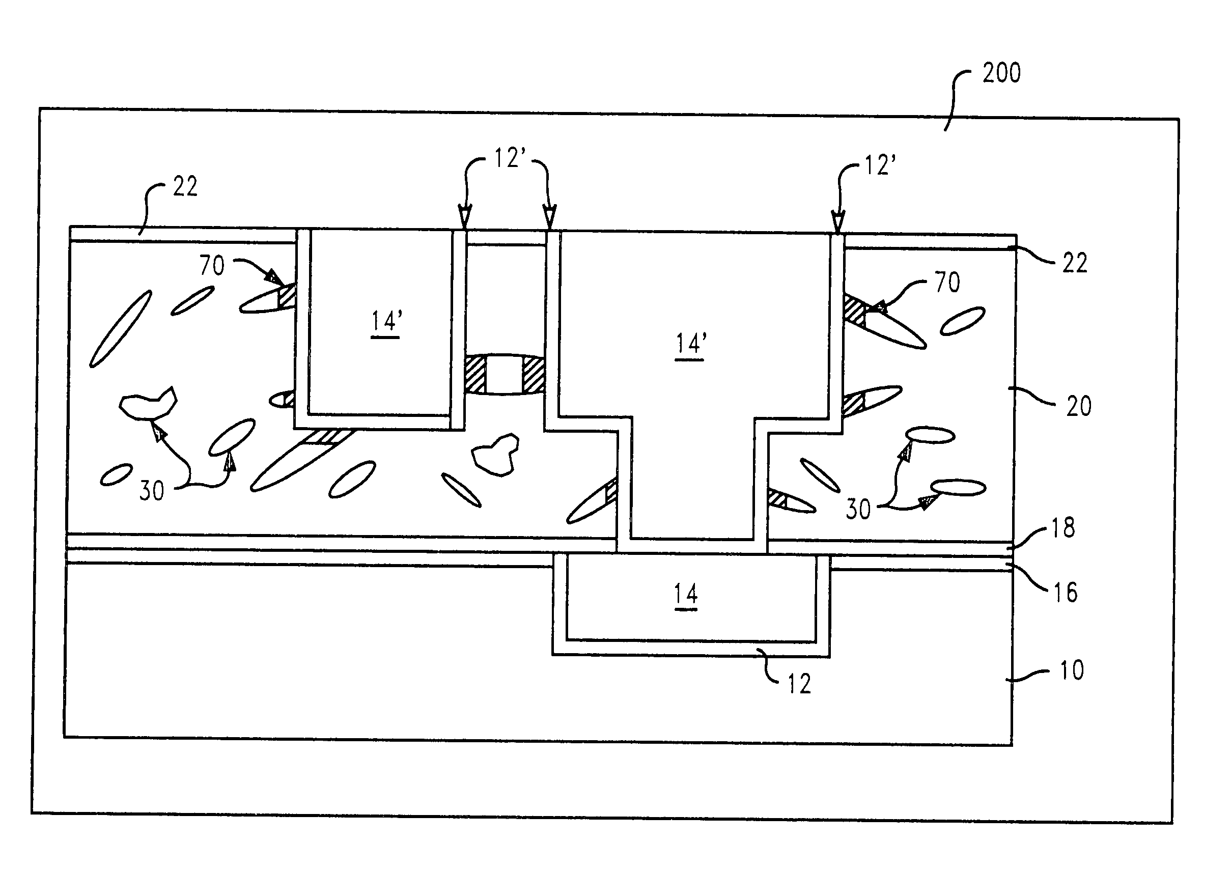
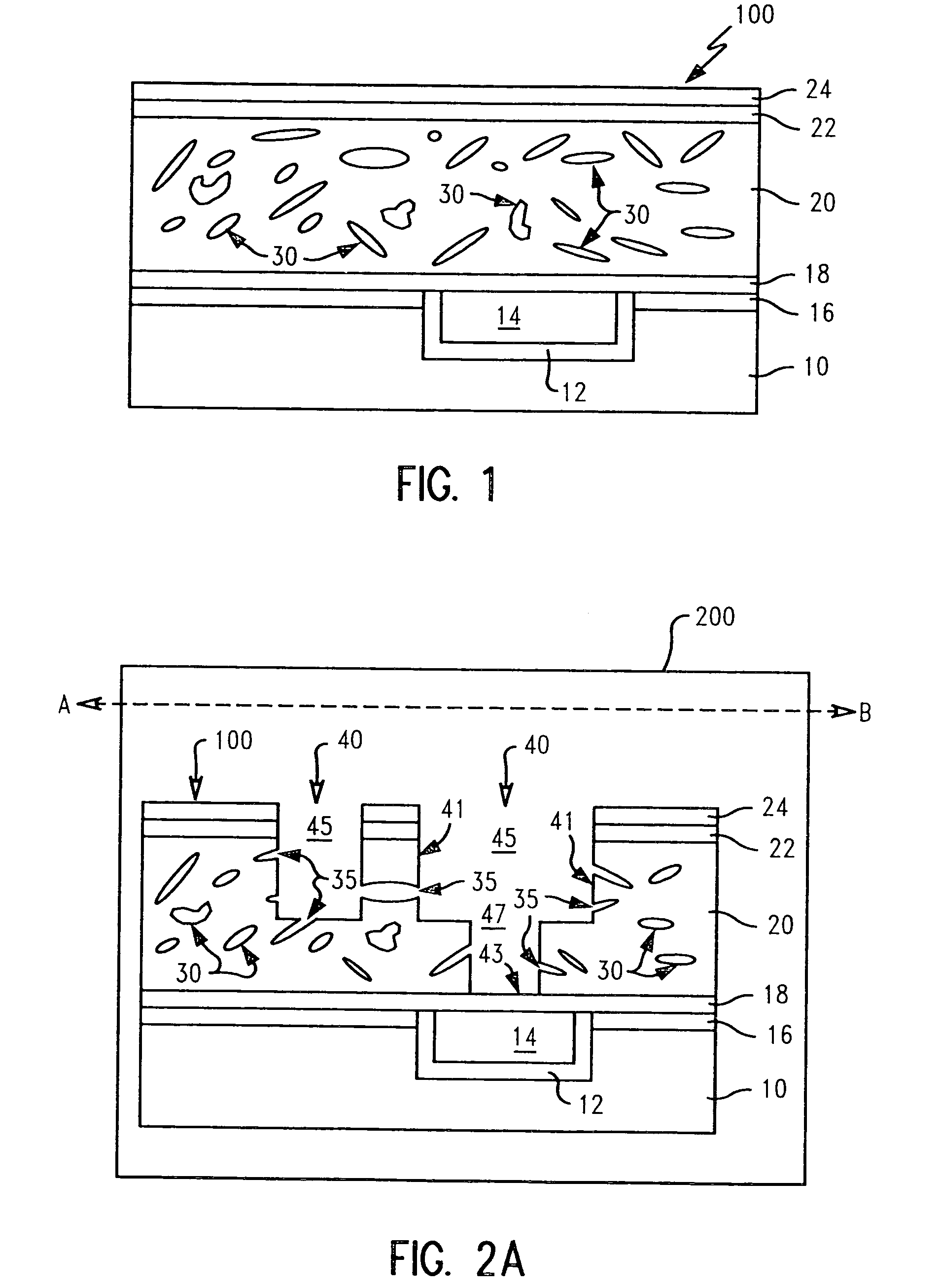
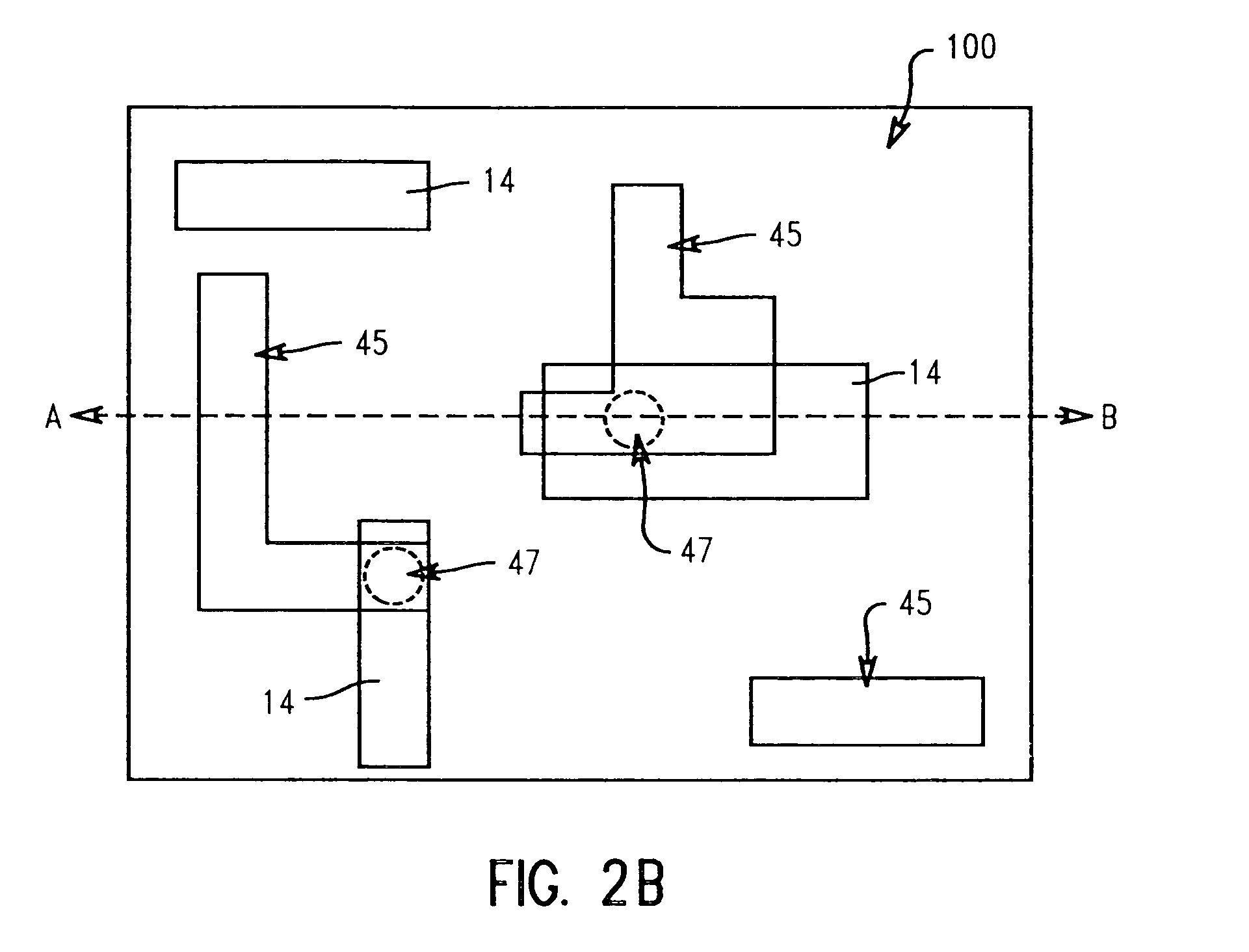
[0061] Dual damascene or single damascene trenches and vias, as discussed above, are formed as known in the art. The present invention provides for closing these exposed pores 35 by first introducing a first reactant, such as, an oxygen-containing surfactant 50 into the chamber, as shown in FIG. 3. For example, water molecules may first be introduced into the chamber. The porous low k dielectric layer may be exposed to the water molecules under processing conditions including pressures ranging from about 1 mTorr to about 7,600 Torr, temperatures ranging from about −50° C. to about 450° C., for a time sufficient to at least allow filling the exposed pores 35 with absorbed water molecules, such as a time ranging from about 10 seconds to about 1 hour.

[0062] By exposing the porous low k dielectric layer to these oxygen-containing surfactant molecules, e.g., water molecules, under the above processing parameters, the oxygen-containing molecules are provided into openings 40 within the p...

example 2

[0072] As an alternative to the above Examples, and without deviating from the novel concept of the invention, a carbon-containing surfactant may be deposited into openings 40 for a time sufficient to allow carbon-containing surfactant molecules absorb within the exposed pores 35 and be retained therein. This carbon-containing surfactant may include, but is not limited to, carbon (C2) Dupanol SP. The carbon-containing surfactant may be introduced into the processing chamber for absorption within the exposed pores 35 under aqueous or supercritical CO2 processing conditions.

[0073] Upon completion of the carbon-containing surfactant deposition process, residual deposited carbon-containing surfactant is removed from the substrate 100, and in particular, from surfaces of the porous low k dielectric layer, including any interior surfaces of openings 40 within porous layer 20. Deposited carbon-containing molecules are removed from interior wall surfaces 41 and bottom surfaces 43 of openin...

example 3

[0077] Also illustrated by FIGS. 3-6, another alternate to the above examples, and again without deviating from the novel concept of the invention, the porous low k dielectric layer may comprise a porous organic material, such as porous SiLK™, whereby ammonia (NH3), TEOS liquid (or vapor), and the like, is readily absorbed by such organic material. Like the examples of the invention described above, NH3 50 may be exposed into openings 40 for a time sufficient to allow NH3 molecules to absorb within the exposed pores 35 and be retained therein. In so doing, if a plasma is used, the NH3 plasma is processed under conditions including pressures of about 1 mTorr to about 100 Torr, temperatures of about −50° C. to about 450° C., and a time ranging from about 10 seconds to about 1 hour.

[0078] Any excess undesired NH3 is then removed from surfaces of the porous layer 20, and in particular, from interior walls and bottoms of openings 40 within porous layer 20, such as by annealing or exposu...


PUM

PropertyMeasurementUnit
thicknessaaaaaaaaaa
dielectric constantaaaaaaaaaa

Abstract

Methods and structures having pore-closing layers for closing exposed pores in a patterned porous low-k dielectric layer, and optionally a reactive liner on the low-k dielectric. A first reactant is absorbed or retained in exposed pores in the patterned dielectric layer and then a second reactant is introduced into openings such that it enters the exposed pores, while first reactant molecules are simultaneously being outgassed. The second reactant reacts in-situ with the outgassed first reactant molecules at a mouth region of the exposed pores to form the pore-closing layer across the mouth region of exposed pores, while retaining a portion of each pore's porosity to maintain characteristics and properties of the porous low-k dielectric layer. Optionally, the first reactant may be adsorbed onto the low-k dielectric such that upon introduction of the second reactant into the patterned dielectric openings, a reactive liner is also formed on the low-k dielectric.

Description

BACKGROUND OF INVENTION [0001] The present invention relates to semiconductor devices and, in particular, to structures and methods for closing exposed pores in a patterned low-k dielectric prior to metallization. [0002] Because of continuing decreases in sizes of integrated circuits (IC) and circuit components in semiconductor chips, there are a number of interconnect wiring challenges facing the technical community over the next few technology generations. Among these challenges include the electrically conductive interconnects being placed closer together vertically, as well as reduction of the horizontal spacing between the electrically conductive interconnects. However, both of these features of smaller ICs result in an undesirable increase in capacitance between conductive portions of the IC, which in turn, results in loss of speed of the IC and increased cross-talk. [0003] In addressing the above problems, prior art has focused on replacing conventional SiO2 dielectric materi...

Claims


Application Information

Patent Timeline
Patent Type & Authority Applications(United States)
IPC IPC(8): H01L21/31H01L21/3105H01L21/311H01L21/316H01L21/469H01L21/4763H01L21/768
CPCH01L21/02107H01L21/76868H01L21/02337H01L21/0234H01L21/02362H01L21/3105H01L21/31116H01L21/31695H01L21/76802H01L21/76807H01L21/7682H01L21/76826H01L21/76831H01L21/76843H01L21/76844H01L21/02203
Inventor COONEY, EDWARD C. IIIFITZSIMMONS, JOHN A.GAMBINO, JEFFREY P.LUCE, STEPHEN E.MCDEVITT, THOMAS L.NICHOLSON, LEE M.STAMPER, ANTHONY K.
Owner ALSEPHINA INNOVATIONS INC
Why Eureka
Try Eureka