Method for processing interior of vapor phase deposition apparatus, method for depositing thin film and method for manufacturing semiconductor device

a technology of vapor phase deposition apparatus and interior, which is applied in the direction of chemical vapor deposition coating, coating, transistor, etc., can solve the problems of reducing the efficiency of ti film nitridation on the interior wall or shower head of the chamber, and achieving the effect of reducing the number of ti film flaking, improving the production efficiency of ti film, and improving the quality

Inactive Publication Date: 2005-12-08
RENESAS ELECTRONICS CORP
View PDF2 Cites 6 Cited by
  • Summary
  • Abstract
  • Description
  • Claims
  • Application Information

AI Technical Summary

Benefits of technology

[0036] According to such process, since the immobilized material is all at once flaked off in every time after a plurality of implementations of the immobilizing the unreacted organic compound are carried out, the throughput per unit time can be increased. Thus, the production efficiency for the thin film is stably improved.
[0037] According to the present invention, since the unreacted organic compound derived from the source gas remained in the interior of the vapor phase deposition apparatus is immobilized by using the reactive gas, the thin film-having higher quality can be stably formed with higher productive efficiency.

Problems solved by technology

Firstly, the technique described in Japanese Patent Laid-Open No. 2000-277,459 involves, in the first place, nitriding the Ti film on the chamber interior wall or on the shower head during the deposition process, and thus it is difficult to employ the technique without any modification to a cleaning process that conducts a cleaning process after unloading the wafer from the interior of the vapor phase deposition apparatus.
Further, since the nitriding reaction is a chemical reaction that is not very reactive, there is a problem of providing lower efficiency for the nitridation of the Ti film on the chamber interior wall or shower head.
In addition, since the nitridation is conducted during the deposition process, the deposition of the Ti film onto the chamber interior wall and the immobilization of the Ti film by the nitridation are not compatible, and thus it is difficult to provide a sufficient prevention for the Ti film being flaked off.
Secondly, in the technique described in Japanese Patent Laid-Open No. 2002-134,488, concerning an unreacted compound that produces a fluorinated compound having relatively lower vapor pressure by a fluorinating reaction therewith, such type of unreacted compound is chemically reacted to form a chemical compound having relatively lower vapor pressure even if fluorine radical ion is introduced therein, and therefore it is difficult to remove such chemical compound by vaporizing thereof.

Method used


Image

  • Method for processing interior of vapor phase deposition apparatus, method for depositing thin film and method for manufacturing semiconductor device
  • Method for processing interior of vapor phase deposition apparatus, method for depositing thin film and method for manufacturing semiconductor device
  • Method for processing interior of vapor phase deposition apparatus, method for depositing thin film and method for manufacturing semiconductor device

Examples


first embodiment

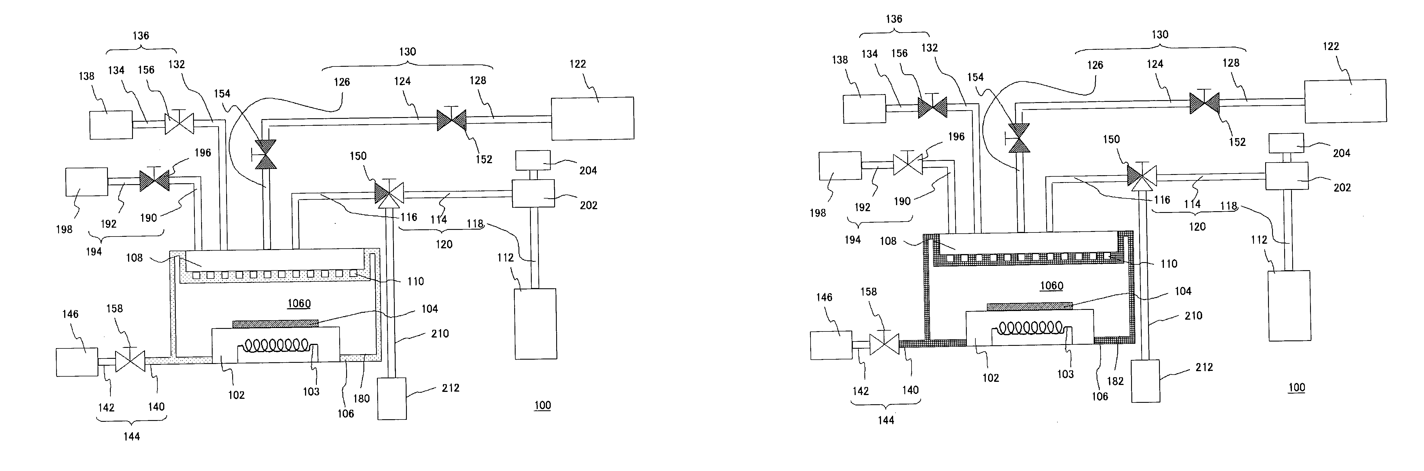
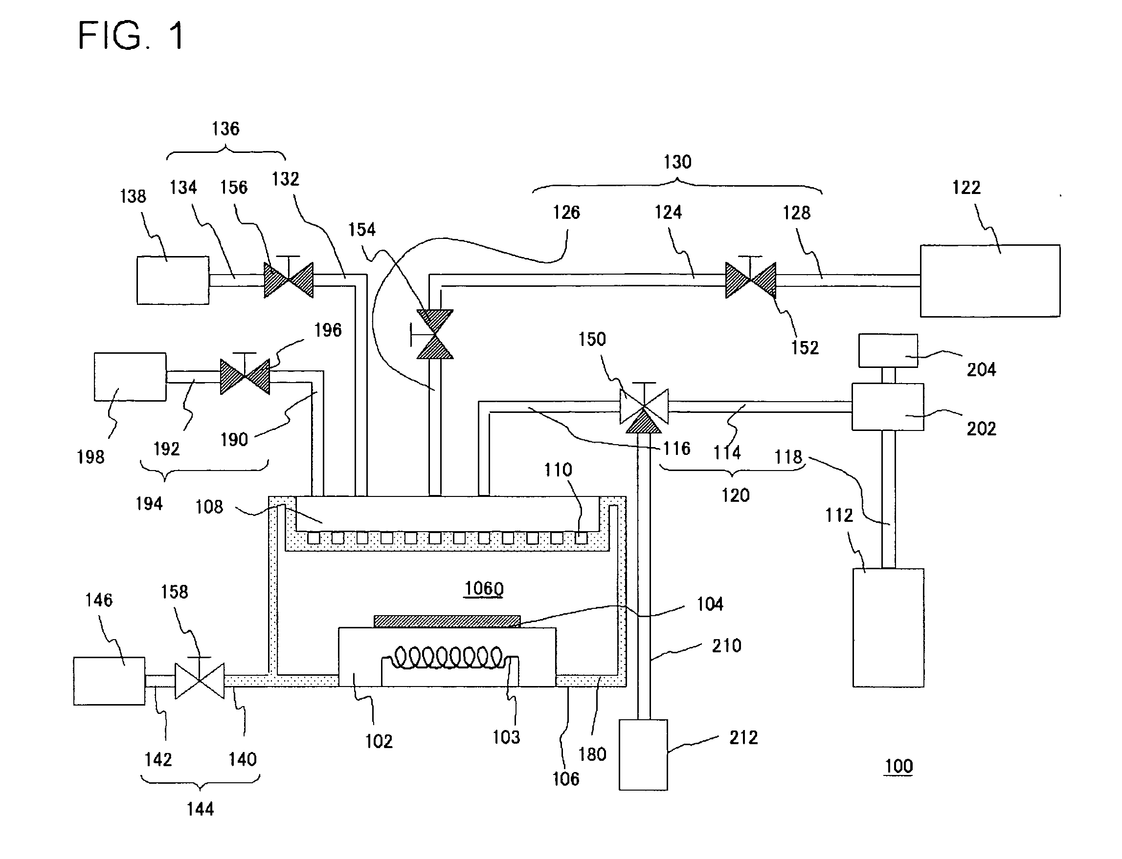
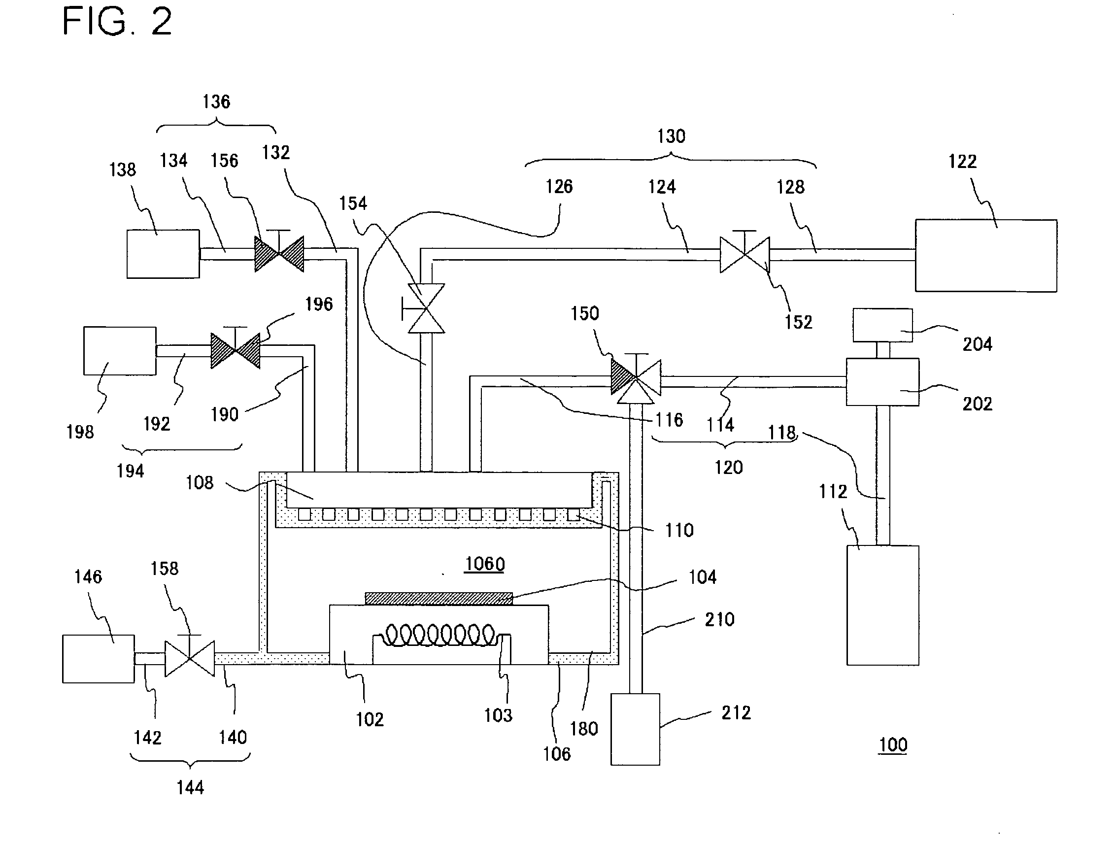
[0053]FIG. 1 is a schematic cross sectional view of a vapor phase deposition apparatus 100 of an embodiment according to the present invention, illustrating a deposition of a thin film with a first source gas.

[0054] A method for processing an interior of the vapor phase deposition apparatus 100 (cleaning method) according to the present embodiment is a method for processing an interior of the vapor phase deposition apparatus 100, which is conducted after carrying out a deposition of a thin film (after forming a metal compound film on a wafer 104 on a support 102) by employing an organic source material (a source gas including Zr or Hf) transported through a source material container 112 and a source material supplying piping 120 into the interior of the vapor phase deposition apparatus (vapor phase deposition apparatus 100), and comprises introducing a reactive gas such as oxidizing gas and the like in the interior of the vapor phase deposition apparatus 100 through an oxidizing ga...

second embodiment

[0131] In the present embodiment, a proper amount of a nitriding gas such as ammonia or nitrogen is employed in addition to the oxidizing gas such as O3 gas as the reactive gas for immobilizing the unreacted organic compound 180 during the oxidation process, to immobilize the unreacted organic compound 180 containing ZrOxCyNzHw by decarbonizing from molecule of the unreacted organic compound 180. Here, a point that is not particularly described in the present embodiment is similar to a point described in the first embodiment. The vapor phase deposition apparatus 100 described in the first embodiment shown in FIG. 1 may be employed for the vapor phase deposition apparatus of the present embodiment.

[0132] As such, the nitriding gas such as NH3 may be employed in addition to the oxidizing gas such as O3 gas to oxynitriding the unreacted organic compound 180, thereby effectively immobilizing the unreacted organic compound.

[0133] In this occasion, when the oxidizing gas such as O3 gas ...

third embodiment

[0144] The present embodiment relates to a method for forming a thin film by using an organic source material containing a heavy metal except Hf or Zr. The method for depositing a thin film according to the present embodiment is the substantially same as the method described in the first embodiment or the second embodiment except the following points.

[0145] While in the above-described embodiment, various types of amino acids containing TEMAZ or the like as a source gas is employed, other source gas having lower vapor pressure may also be employed. Also in such case, since the unreacted compound of a source gas can be immobilized according to the method for depositing the metal compound film of the present invention, the high dielectric constant film having higher quality can similarly be obtained with higher stability.

[0146] More specifically, organic source materials containing a heavy metal such as La, Pr, Pb, Sr, Ba, Cu, Ti, Bi and the like and having a vapor pressure of equal...


PUM

PropertyMeasurementUnit
pressureaaaaaaaaaa
pressureaaaaaaaaaa
pressureaaaaaaaaaa

Abstract

A method for depositing a metal compound film on the wafer by using a vapor phase deposition apparatus 100, comprising: forming a thin film on the wafer in an interior of the vapor phase deposition apparatus 100 by introducing a source gas for the metal compound film containing Hf or Zr; unloading the wafer having the metal compound film formed thereon from the interior of the vapor phase deposition apparatus 100; introducing a reactive gas in the interior of the vapor phase deposition apparatus 100 to immobilize the unreacted organic compound 180 derived from the source gas remained in the interior of the vapor phase deposition apparatus 100; loading another wafer in the interior of the vapor phase deposition apparatus 100; and depositing metal compound film on another wafer by further introducing the source gas in the interior of the vapor phase deposition apparatus 100, in the condition that the unreacted organic compound 180 exists therein as an immobilized form, is presented.

Description

[0001] This application is based on Japanese patent application NO. 2004-164126, the content of which is incorporated hereinto by reference. BACKGROUND OF THE INVENTION [0002] 1. Field of the Invention [0003] The present invention relates to a method for processing an interior of a vapor phase deposition apparatus, a method for depositing a thin film and a method for manufacturing a semiconductor device. [0004] 2. Related Art [0005] In recent years, various innovations on techniques for inhibiting a generation of particles in a metal compound film are actively made for the purpose of providing a stable formation of a metal compound film having improved quality by employing a vapor phase deposition apparatus. Typical example of such techniques includes a technique disclosed in Japanese Patent Laid-Open No. 2000-277,459. Japanese Patent Laid-Open No. 2000-277,459 describes a technique for nitriding a Ti film disposed on a chamber interior wall or a shower head during a deposition proc...

Claims


Application Information

Patent Timeline
Patent Type & Authority Applications(United States)
IPC IPC(8): C23C16/00C23C16/44C23C16/30C23C16/40H01L21/31H01L21/8242H01L27/108H01L29/78
CPCC23C16/308C23C16/45531C23C16/405
Inventor YAMAMOTO, TOMOE
Owner RENESAS ELECTRONICS CORP
Why Eureka
Try Eureka