Semiconductor device

a technology of semiconductor substrates and semiconductors, applied in the direction of semiconductor devices, basic electric elements, electrical equipment, etc., can solve the problems of reducing the effective epitaxial thickness, and achieve the effects of reducing the resistance of the semiconductor substrate, and reducing the resistan

Inactive Publication Date: 2005-12-08
RENESAS ELECTRONICS CORP
View PDF5 Cites 34 Cited by
  • Summary
  • Abstract
  • Description
  • Claims
  • Application Information

AI Technical Summary

Benefits of technology

[0014] According to the present invention, since the first conductivity type impurity contained in the semiconductor substrate and the second conductivity type impurity contained in the second conductivity type impurity-implanted layer attract each other by coulomb force, an extending of the semiconductor substrate can be prevented. Accordingly, an increase of the film thickness for the effective epitaxial thickness can be achieved, and thus a semiconductor device comprising a field effect transistor having larger drain-source breakdown voltage and smaller drain-source capacitance can be achieved.
[0016] The semiconductor devices according to the present invention may further have a configuration, in which the first conductivity type impurity may include As or Sb. Resistance of the semiconductor substrate can be reduced by implanting As or Sb, which has comparatively smaller resistivity, as the first conductivity type impurity into the semiconductor substrate. Accordingly, the semiconductor device comprising the field effect transistor having the back surface source-grounding structure comprising the semiconductor substrate having lower resistance can be achieved. In addition, the extending of the semiconductor substrate can be further inhibited by forming the second conductivity type impurity-implanted layer on the semiconductor substrate implanted with As or Sb having comparatively smaller diffusion coefficient. Therefore, further increase in the film thickness for the effective epitaxial thickness can be achieved. As a result, the semiconductor device comprising the field effect transistor having higher drain-source breakdown voltage and lower drain-source capacitance can be achieved.

Problems solved by technology

Further, a diffusion of an impurity into a substrate is often conducted in order to contact the source with the back surface of the substrate, while an unwanted extending of the substrate is occurred by the diffusion of the impurity, thereby reducing the effective epitaxial thickness.

Method used


Image

  • Semiconductor device
  • Semiconductor device
  • Semiconductor device

Examples


Embodiment Construction

[0028] The invention will be now described herein with reference to illustrative embodiments. Those skilled in the art will recognize that many alternative embodiments can be accomplished using the teachings of the present invention and that the invention is not limited to the embodiments illustrated for explanatory purposed.

[0029] Embodiments according to the present invention will be described as follows in further detail, in reference to the annexed figures. In all figures, identical numeral is assigned to an element commonly appeared in the figures, and the detailed description thereof will not be presented.

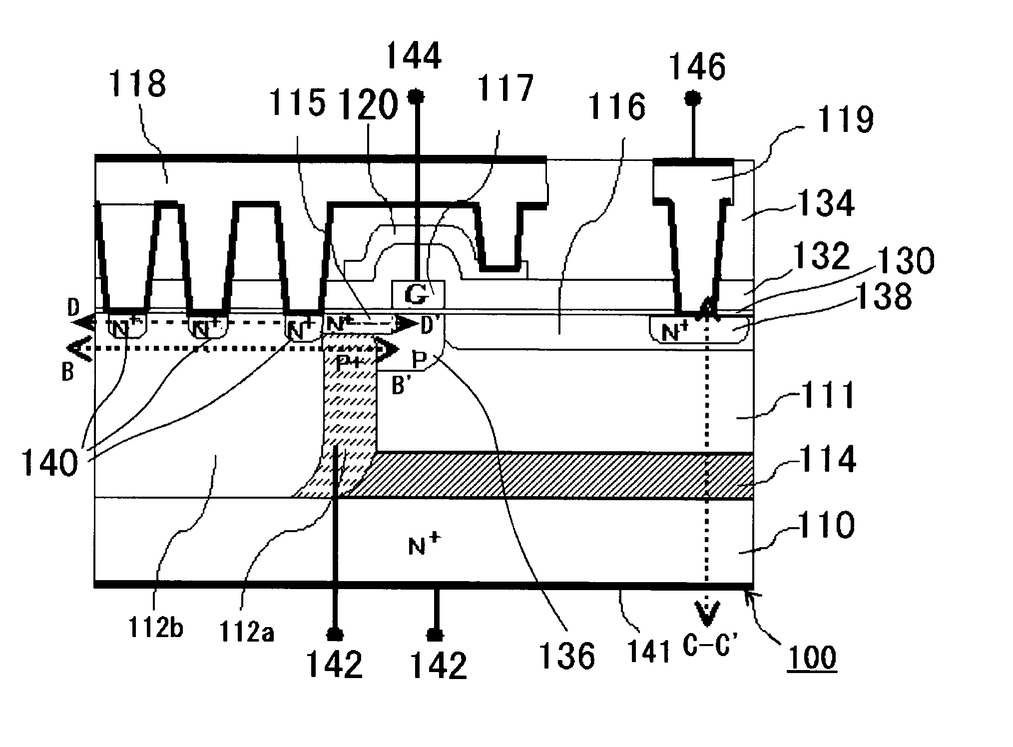
[0030] While the present embodiment is intended to describe, for example, an N-channel lateral MOSFET employing an N-type impurity as a first conductivity type impurity and employing a P-type impurity as a second conductivity type impurity, similar description can also be made for a P-channel lateral MOSFET, as taking the reversed conductivity types of the impurities.

[0031...


PUM


Abstract

The semiconductor device comprises: a semiconductor substrate (N+ substrate 110) containing a first conductivity type impurity implanted therein; a second conductivity type impurity-implanted layer (P+ implanted layer 114) at relatively high concentration, formed on the semiconductor substrate (N+ substrate 110); a second conductivity type impurity epitaxial layer (P− epitaxial layer 111) at relatively low concentration, formed on the second conductivity type impurity-implanted layer (P+ implanted layer 114); and a field effect transistor 100 (N-channel type lateral MOSFET 100)composed of a pair of impurity diffusion regions (N+ source diffusion layer 115 and N− drain layer 116) provided in the second conductivity type impurity epitaxial layer (P− epitaxial layer 111) and a gate electrode 117 provided over a region sandwiched with the pair of impurity diffusion regions (N+ source diffusion layer 115 and N− drain layer 116).

Description

[0001] This application is based on Japanese patent application NO. 2004-170536, the content of which is incorporated hereinto by reference. BACKGROUND OF THE INVENTION [0002] 1. Field of the Invention [0003] The present invention relates to a semiconductor device. [0004] 2. Related Art [0005] In field effect transistors (FETs) such as a lateral power metal oxide semiconductor field effect transistor (MOSFET) having a source electrode on a back surface (a back surface source), a thickness of an effective epitaxial layer (hereinafter referred to as “effective epitaxial thickness”) is considerably influential on a drain-source breakdown voltage (BVdss) and a drain-source capacitance (Cds), and it is preferable to have thicker effective epitaxial thickness to increase the drain-source breakdown voltage and reduce the drain-source capacitance. [0006] Further, a diffusion of an impurity into a substrate is often conducted in order to contact the source with the back surface of the substr...

Claims


Application Information

Patent Timeline
Patent Type & Authority Applications(United States)
IPC IPC(8): H01L21/336H01L29/06H01L29/10H01L29/417H01L29/78
CPCH01L29/0696H01L29/1045H01L29/1083H01L29/402H01L29/7835H01L29/4175H01L29/41758H01L29/66659H01L29/41725
Inventor TSUBAKI, SHIGEKI
Owner RENESAS ELECTRONICS CORP
Why Eureka
Try Eureka