Semiconductor device having stress and its manufacture method

a technology of stress and semiconductors, applied in the direction of semiconductor devices, electrical devices, transistors, etc., can solve the problem of difficult control of the etching process of forming contact holes, and achieve the effect of increasing stress (strain) applied to the channel region and increasing stress

Active Publication Date: 2005-12-08
FUJITSU SEMICON LTD
View PDF6 Cites 70 Cited by
  • Summary
  • Abstract
  • Description
  • Claims
  • Application Information

AI Technical Summary

Benefits of technology

[0021] The source / drain regions on both sides of the gate electrode are dug from the surfaces thereof to form the recess regions, and the nitride film is formed burying the recess regions. Stress applied to the channel region can therefore be increased. The stress (strain) applied to the channel region can be increased without thickening the nitride film and without narrowing the side wall spacer width.

Problems solved by technology

As a nitride film used as an etching stopper film is thickened, it becomes difficult to control an etching process of forming a contact hole.

Method used


Image

  • Semiconductor device having stress and its manufacture method
  • Semiconductor device having stress and its manufacture method
  • Semiconductor device having stress and its manufacture method

Examples


first embodiment

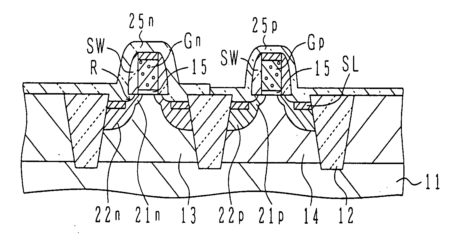
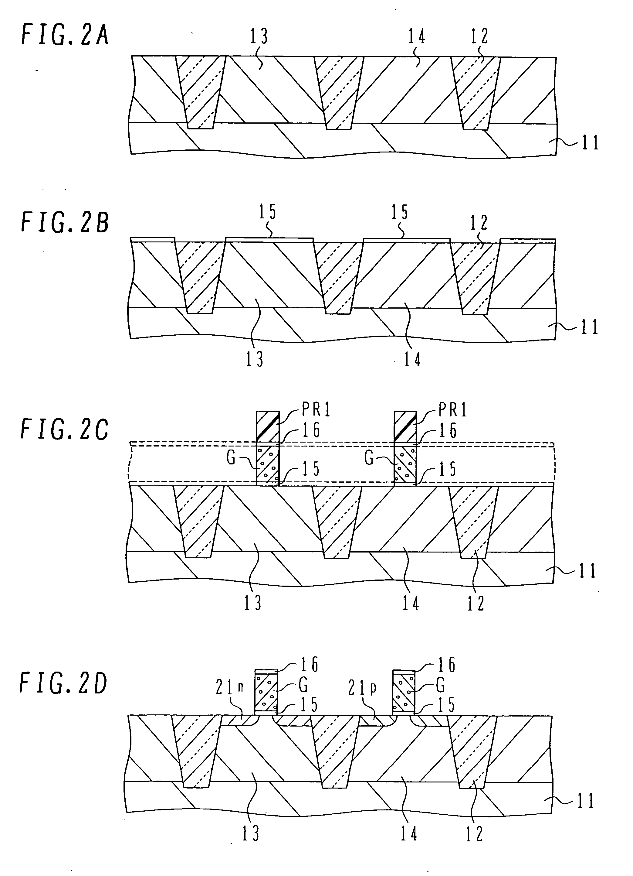
[0032]FIG. 1A is a schematic cross sectional view showing the structure of a CMOS semiconductor device according to the invention. A shallow trench as an element isolation region is formed in a surface layer of a p-type silicon substrate 11, and an insulating film such as an oxide film is filled in the trench to form a shallow trench isolation (STI) region 12.

[0033] Well forming impurities are implanted in active regions defined by the STI region 12 to form a p-type well 13 for an n-channel MOSFET and an n-type well 14 for a p-channel MOSFET. A gate insulating film 15 is formed on the surface of the active region, and a polysilicon layer as a gate electrode film is deposited on the gate insulating film. The polysilicon layer and gate insulating film are patterned to form an insulated gate electrode structure.

[0034] In the p-type well 13, n-type impurities are implanted shallowly to form an n-type extension region 21n, and in the n-type well 14, p-type impurities are implanted shall...

second embodiment

[0068]FIGS. 3A to 3G are cross sectional views illustrating a CMOS semiconductor device manufacture method the method using a simplified process. First, by using the processes shown in FIGS. 2A to 2E, the insulated gate electrode structure, side wall spacers and extension regions are formed.

[0069] As shown in FIG. 3A, a photoresist mask 31 is formed covering a p-channel MOSFET region and exposing an n-channel MOSFET region in an opening of the photoresist mask 31.

[0070] As shown in FIG. 3B, in the state that the p-channel MOSFET region is covered with the photoresist mask 31, similar to the process shown in FIG. 2F, RIE is performed to form recess regions 32 only in the n-channel MOSFET region, the recess regions being formed by digging the silicon substrate outside of the side wall spacers from the surfaces of the substrate.

[0071] As shown in FIG. 3C, similar to the process shown in FIG. 2G, isotropic etching such as wet etching using HCl is performed to form recess regions 33 o...


PUM


Abstract

A semiconductor device has: active regions including a p-type active region; an insulated gate electrode structure formed on each of the active regions, and having a gate insulating film and a gate electrode formed thereon; side wall spacers formed on side walls of the insulated gate electrode structures; source / drain regions having extension regions having the opposite conductivity type to that of the active region and formed on both sides of the insulated gate electrode structures and source / drain diffusion layers having the opposite conductivity type and formed in the active regions outside of the side wall spacers; first recess regions formed by digging down the n-type source / drain regions in the p-type active region from surfaces of the n-type source / drain regions; and a first nitride film having tensile stress formed covering the p-type active region and burying the first recess regions.

Description

CROSS REFERENCE TO RELATED APPLICATION [0001] This application is based on and claims priority of Japanese Patent Application No. 2004-170037 filed on Jun. 8, 2004, the entire contents of which are incorporated herein by reference. BACKGROUND OF THE INVENTION [0002] A) Field of the Invention [0003] The present invention relates to a semiconductor device and its manufacture method, and more particularly to a semiconductor device having a nitride film on a semiconductor substrate as an etching stopper film and to its manufacture method. [0004] B) Description of the Related Art [0005] A mobility of charge carriers in semiconductor is influenced by stress. For example, a mobility of electrons in silicon increases as a tensile stress increases, whereas it decreases as the tensile stress decreases. Conversely, a mobility of holes in silicon increases as a compressive stress increases, whereas it decreases as the compressive stress decreases. [0006] Manufacture processes for a semiconducto...

Claims


Application Information

Patent Timeline
Patent Type & Authority Applications(United States)
IPC IPC(8): H01L21/336H01L21/8238H01L27/092H01L29/76H01L29/78
CPCH01L21/823807H01L21/823814H01L29/7843H01L29/66636H01L29/7842H01L29/665
Inventor PIDIN, SERGEY
Owner FUJITSU SEMICON LTD
Why Eureka
Try Eureka