
Eureka
For R&D, Eureka makes reading and utilizing patents & technical documents easy.
Eureka AIR
Designed for self-driven R&D workflows. Generate viable solutions, solve complex R&D challenges, empower your innovation with AI.

Eureka Materials
Designed for material experts only. Revolutionize your material R&D, from search, analyze, to developing new materials.

TechResearch
Generate reliable direction feasibility study reports for your R&D in just a few steps.

TechSeek
Discover and master advanced knowledge NOW. Basics, ideas, possibilities, all at once.

TechMind
As an expert in R&D Theories, TechMind can generates customized viable solutions instantly.

TechRisk
Analyze your overall solution with one click, know your potential R&D risks in advance.

TechMonitor
Get weekly tech updates, stay abreast of the latest tech innovations and key insights.
Pressure sensitive adhesive sheet for use in semiconductor working and method for producing semiconductor chip
- Summary
- Abstract
- Description
- Claims
- Application Information
AI Technical Summary
Benefits of technology
Problems solved by technology
Method used
Image

Examples
example 1
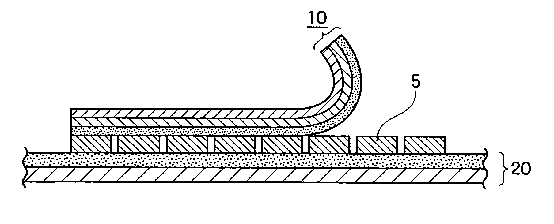
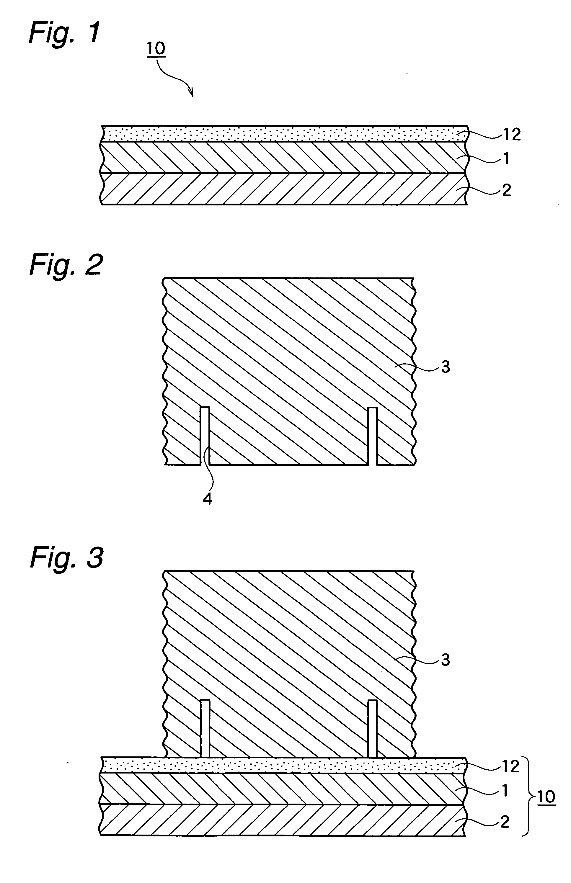
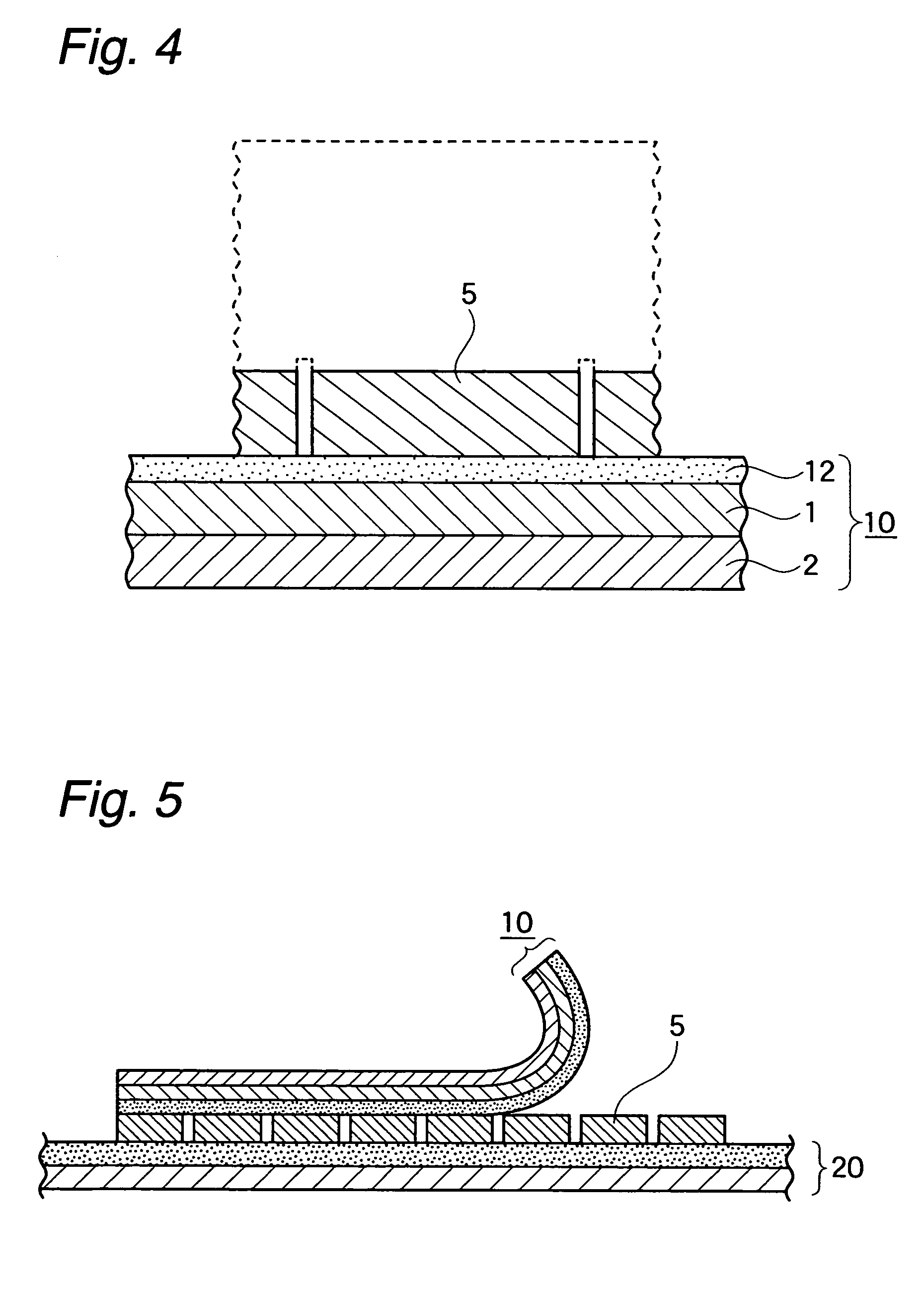
[0081] Rigid substrate: polyethylene terephthalate (PET) film having a thickness of 25 μm.
[0082] Vibration relaxation layer: a composition including 60 parts by weight of bifunctional urethane acrylate type oligomer having a weight average molecular weight of 8100 (trade name: UX-3301; manufactured by Nippon Kayaku Co., Ltd.), 40 parts by weight of dicyclopentanyl acrylate, 4.0 parts by weight of 1-hydroxycyclohexyl phenyl ketone (trade name: IRGACURE™ 184; Ciba Specialty Chemicals) as a phtopolymerization initiator was applied on one face of the rigid substrate such that it had a thickness of 45 μm after UV cured and, then, cured by a UV irradiation, to thereby form a vibration relaxation layer.
[0083] Pressure sensitive adhesive layer: a pressure sensitive adhesive composition comprising 100 parts by weight of acrylic pressure sensitive adhesive (copolymer of 85 parts by weight of butyl acrylate, 9 parts by weight of methyl methacrylate, 5 parts by weight of hydroxyethyl acrylate...
example 2
[0086] A pressure sensitive adhesive sheet was prepared in a same manner as in Example 1 except that, in the pressure sensitive adhesive layer, the composition was changed into that including 100 parts by weight of acrylic pressure sensitive adhesive (copolymer (weight average molecular weight: 600000) of 90 parts by weight of n-butyl acrylate and 10 parts by weight of acrylic acid), 120 parts by weight of urethane acrylate type oligomer having a weight average molecular weight of 5000, 2.0 parts by weight of a photopolymerization initiator (trade name: IRGACURE™ 184; manufactured by Ciba Specialty Chemicals) and 2 parts by weight of an adduct of tolylene diisocyanate and trimethylol propane as a curing agent and, also, the thickness of thereof after cured was changed into 200 μm (elastic modulus at 23° C. prior to energy ray curing: 1.5×10⁵ Pa). The thus-obtained pressure sensitive adhesive sheet was applied on a half-cut mirror face of the wafer and, then, subjected to the back fa...
example 3
[0087] A pressure sensitive adhesive sheet was prepared in a same manner as in Example 1 except that the rigid substrate was changed into a polyethylene terephthalate film having a thickness of 125 μm. The thus-obtained pressure sensitive adhesive sheet was applied on a half-cut mirror face of the wafer and, then, subjected to the back face grinding test. The results are shown in Table 1.
PUM
 Abstract
Description
Claims
Application Information
 - R&D Engineer
- R&D Manager
- IP Professional
- Industry Leading Data Capabilities
- Powerful AI technology
- Patent DNA Extraction
Browse by: Latest US Patents, China's latest patents, Technical Efficacy Thesaurus, Application Domain, Technology Topic, Popular Technical Reports.
© 2024 PatSnap. All rights reserved.Legal|Privacy policy|Modern Slavery Act Transparency Statement|Sitemap|About US| Contact US: help@patsnap.com