Substrate structure integrated with passive components

a technology of passive components and substrates, applied in the association of semiconductor/solid-state devices, printed circuit non-printed electric components, electrical apparatus construction details, etc., can solve the problems of increasing the overall size of the semiconductor package, increasing the trace routability of the substrate, and undetectedly enlarging the package size and complicating the fabrication process of the semiconductor package. , to achieve the effect of reducing fabrication costs, reducing use, and simplifying fabrication processes

Inactive Publication Date: 2005-12-08
PHOENIX PRECISION TECH CORP
View PDF8 Cites 26 Cited by
  • Summary
  • Abstract
  • Description
  • Claims
  • Application Information

AI Technical Summary

Benefits of technology

[0025] Therefore, the substrate structure integrated with the passive components according to the present invention only requires a simple fabrication method and eliminates the use of the complex substrate and packaging processes complying with the fabrication of passive components, such that the present invention solves the prior-art drawbacks, and reduces the fabrication cost due to simplification of the fabrication processes, as well as improves flexibility of the trace routability for semiconductor packaging substrates.

Problems solved by technology

In other words, a larger substrate should be used and thus increases the overall size of the semiconductor package.
Along with the requirement of enhanced performance for the semiconductor packages, more passive components are accordingly required, making the surface of the substrate necessary to simultaneously accommodate a plurality of semiconductor chips and numbers of the passive components, and thereby undesirably enlarging the package size and complicating the fabrication processes of the semiconductor packages.
Moreover, the above passive components are respectively incorporated on the substrate, which not only raise the trace routability on the substrate but also make the fabrication processes of the substrate and the package more complex, thus not considered cost-effective.
In addition, if either the passive component or the substrate is damaged, it would cause the entire semiconductor package to fail, and thus leads to increase in the production cost and the reliability issue.
However, the restriction on locating the passive components confines the flexibility of trace routability on the substrate, and the number of the passive components would be limited if considering the positions of the electrical pads on the substrate.
However, although the integration of film-type passive components in the multi-layer circuit board solves the problems of restriction on trace routability of the circuit board, this integration method is rather complex to implement.
Besides, since the passive components are located between the laminated layers of the circuit board, to achieve different requirements of the electrical characteristics such as resistance and capacitance, a newly designed and laminated multi-layer circuit board must be prepared, which would significantly increase the fabrication and material costs and result in difficulty in managing material stocks.
Therefore, the above integration method for passive components complicates the entire structure of the substrate and the fabrication method thereof, thereby not compliant with the economic concern.
Therefore, the current semiconductor packaging technology cannot perfectly achieve high integration arrangement of electronic elements and electronic circuits in the semiconductor packages to provide satisfactory multiple functions and high efficiency for the electronic products.

Method used


Image

  • Substrate structure integrated with passive components
  • Substrate structure integrated with passive components
  • Substrate structure integrated with passive components

Examples


Embodiment Construction

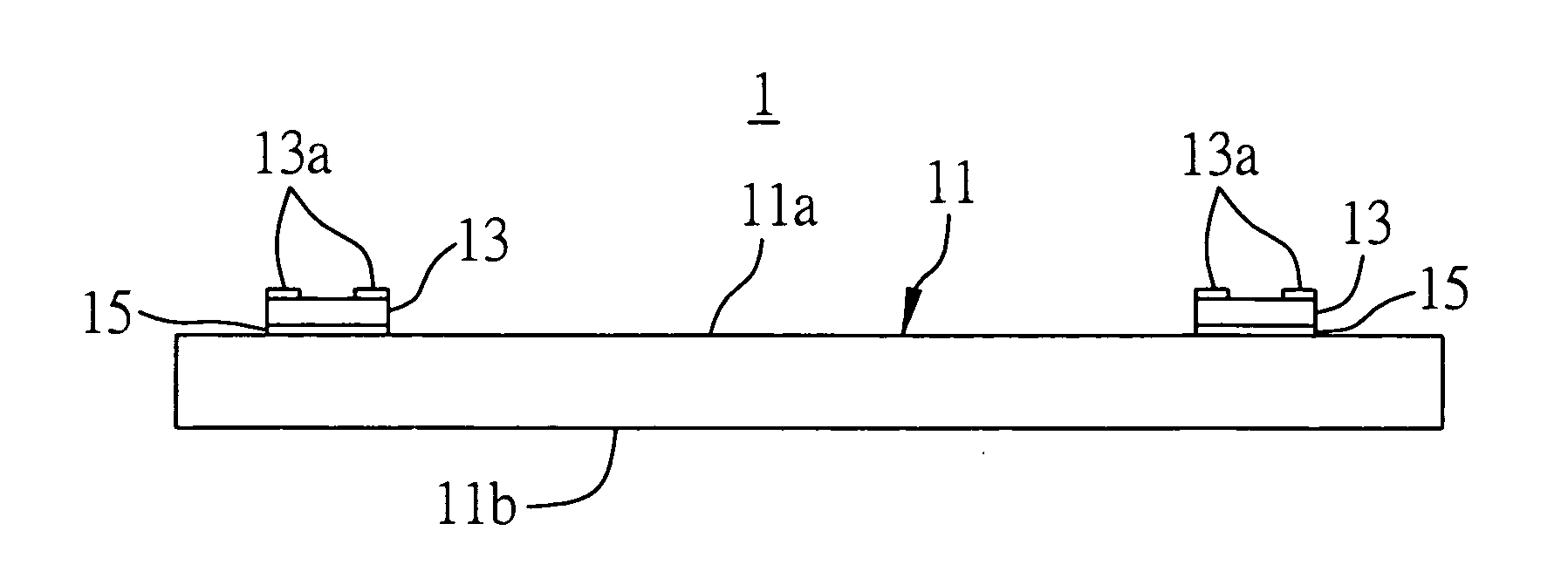
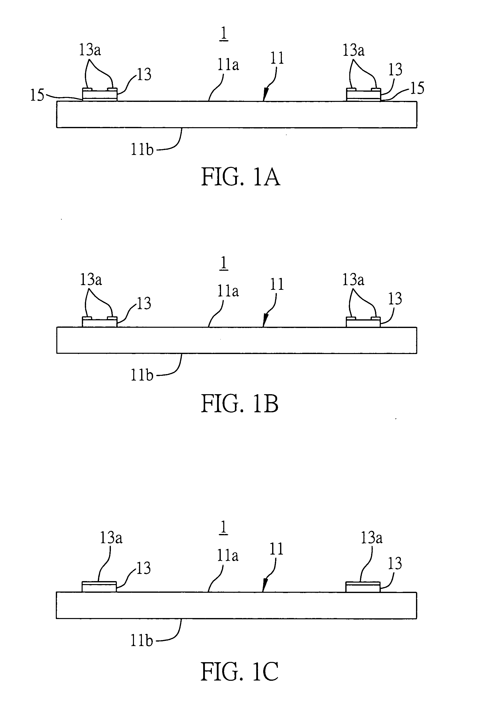
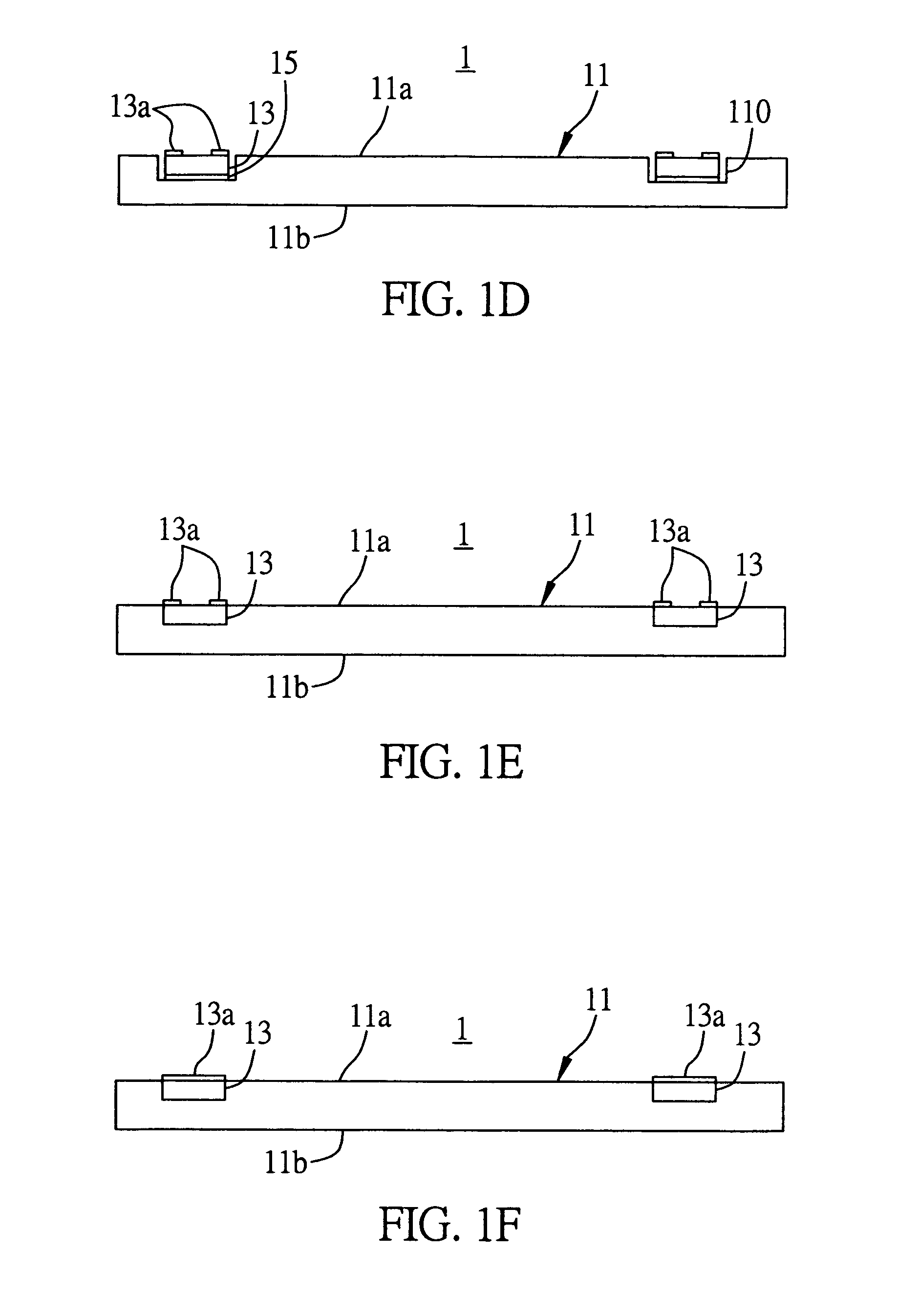
[0036] The preferred embodiments of a substrate structure integrated with passive components proposed in the present invention are described in detail as follows with reference to FIGS. 1 to 9.

[0037]FIGS. 1A to 1F are cross-sectional views of the substrate structure integrated with passive components according to a first preferred embodiment of the present invention.

[0038] Referring to FIG. 1A, the substrate structure 1 comprises a carrier plate 11 having an upper surface 11a and an opposite lower surface 11b, and a plurality of passive components 13 mounted on the upper surface 11a of the carrier plate 11. It should be understood that the passive components 13 are not limited to being located on the upper surface 11a of the carrier plate 11, which can also be disposed on the lower surface 11b of the carrier plate 11 depending on the practical requirement. The passive components 13 can be surface-mounted or chip-type passive components, and the carrier plate 11 can be made of a me...


PUM


Abstract

A substrate structure integrated with passive components is proposed. The substrate structure includes a carrier plate and a plurality of passive components provided on the carrier plate. The carrier plate is formed with at least one cavity for receiving the passive components and at least one opening for receiving electronic elements. Further, a heat sink can be attached to the carrier plate to improve the heat dissipation efficiency. An insulating layer with circuit structures can be formed on the carrier plate to modularize the substrate structure, so as to provide a desirable electrical design of semiconductors carried by the substrate structure.

Description

FIELD OF THE INVENTION [0001] The present invention relates to substrate structures integrated with passive components, and more particularly, to a modularized structure with a plurality of passive components incorporated on a carrier plate for use in a semiconductor package. BACKGROUND OF THE INVENTION [0002] To satisfy the requirements of high integration and miniaturization for semiconductor packages, electronic elements and electronic circuits should also be densely arranged in the semiconductor packages. Accordingly, it usually incorporates passive components such as resistors, capacitors and inductors in the semiconductor packages to improve or stabilize the electrical performance of the electronic products. [0003] At present, with regard to flip-chip, ball grid array (BGA) or wire-bonded semiconductor packages, it is usually to first form patterned conductive traces on the surface of a substrate, and then before packaging, mount passive components for noise elimination or ele...

Claims


Application Information

Patent Timeline
Patent Type & Authority Applications(United States)
IPC IPC(8): H05K3/46H05K1/02H01L23/538H05K1/18H05K7/20
CPCH01L23/5389H01L2224/24227H01L2924/01025H01L2924/09701H05K1/023H05K1/185H05K3/0064H05K3/4602H01L2924/15153
Inventor HSU, SHIH-PING
Owner PHOENIX PRECISION TECH CORP
Why Eureka
Try Eureka