High density interconnect system having rapid fabrication cycle

a high density interconnect and fabrication cycle technology, applied in the field of semiconductor/solid-state device testing/measurement, individual semiconductor device testing, instruments, etc., can solve the problems of time-consuming, several limitations of parallelism correction and verification using precision point vx, and the cost of testing each die is becoming a greater and greater fraction of the total device cost. , to achieve the effect of improving the fabrication cycl

Inactive Publication Date: 2005-12-15
ADVANTEST SINGAPORE PTE LTD
View PDF12 Cites 46 Cited by
  • Summary
  • Abstract
  • Description
  • Claims
  • Application Information

AI Technical Summary

Benefits of technology

[0025] An improved interconnection system and method is described, such as for connectors, socket assemblies and / or probe card systems. An exemplary system comprises a probe card interface assembly for establishing electrical connections to a semiconductor wafer mounted in a semiconductor wafer prober. The probe card interface assembly comprises a mother board having an upper surface and a lower planar mounting surface opposite the upper surface and parallel to the semiconductor wafer, a reference plane defined by a least three points located between the lower surface of the motherboard and the semiconductor wafer, at least one component having an upper mounting surface located below the motherboard mounting surface and a lower mounting surface opposite the upper mounting surface, and a mechanism for adjusting the planarity of the reference plane with respect to the semiconductor wafer. A probe chip having a plurality of spring probes extending there from is mountable and demountable from the probe card interface assembly, without the need for further planarity adjustment. The interconnection structures and methods preferably provide improved fabrication cycles.

Problems solved by technology

With more die to test per wafer and each die having more I / O pads, the cost of testing each die is becoming a greater and greater fraction of the total device cost.
There are, however, several limitations to this method of parallelism correction and verification using Precision Point VX.
First, it is time consuming.
Second, if the measurement is made under simulated tester interface force loading conditions, it may not include all aspects of the mechanical deflection associated with the forces applied during actual operation in a wafer prober.
Third, the measurement may be done at room temperature and may not be indicative of the actual operating temperature which will induce mechanical changes due to the thermal coefficients of the various materials in the probe card assembly.
However, this is problematic because wafer probers are generally used in production environments and such activities may not be desirable.
Additionally, special equipment or tooling may be required which can cause additional complication and chance for error.
In any case, it is an additional burden on the user if it is required to adjust the planarity of the probe tips each time the probe card is moved from one wafer prober to another or from a quality control (QC) test instrument, such as the Precision Point VX to a wafer prober.
As conventional assembly structures and manufacturing methods include such long lead time components, that the resulting fabrication cycle for one or more assemblies is long.

Method used


Image

  • High density interconnect system having rapid fabrication cycle
  • High density interconnect system having rapid fabrication cycle
  • High density interconnect system having rapid fabrication cycle

Examples


Embodiment Construction

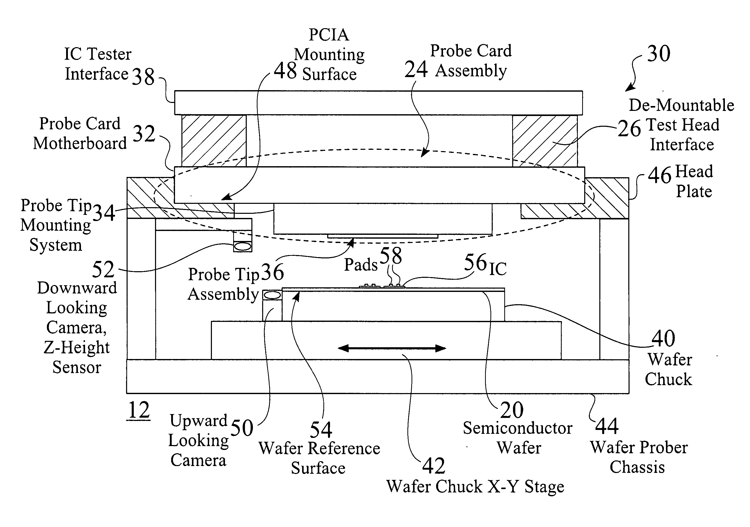
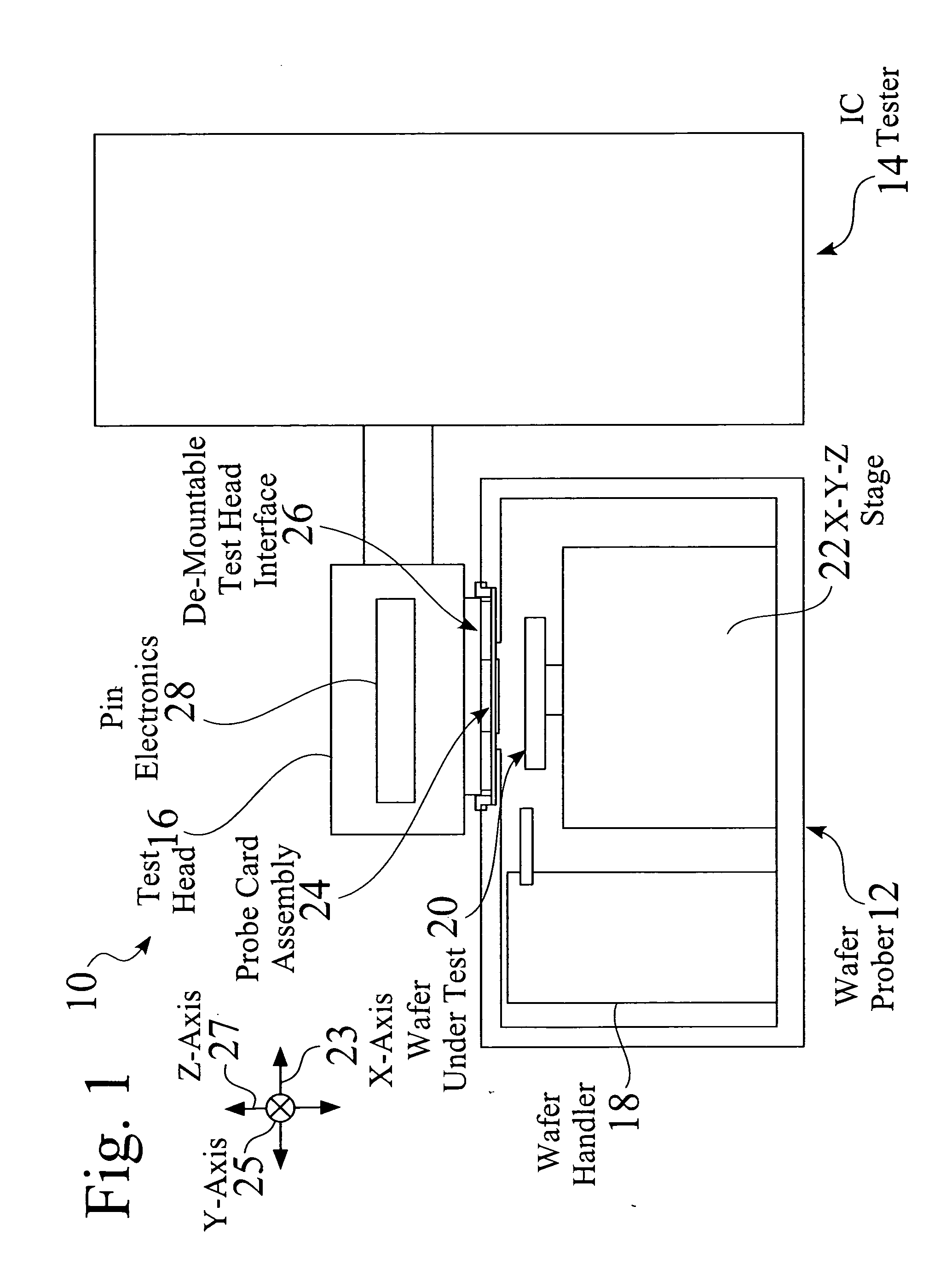
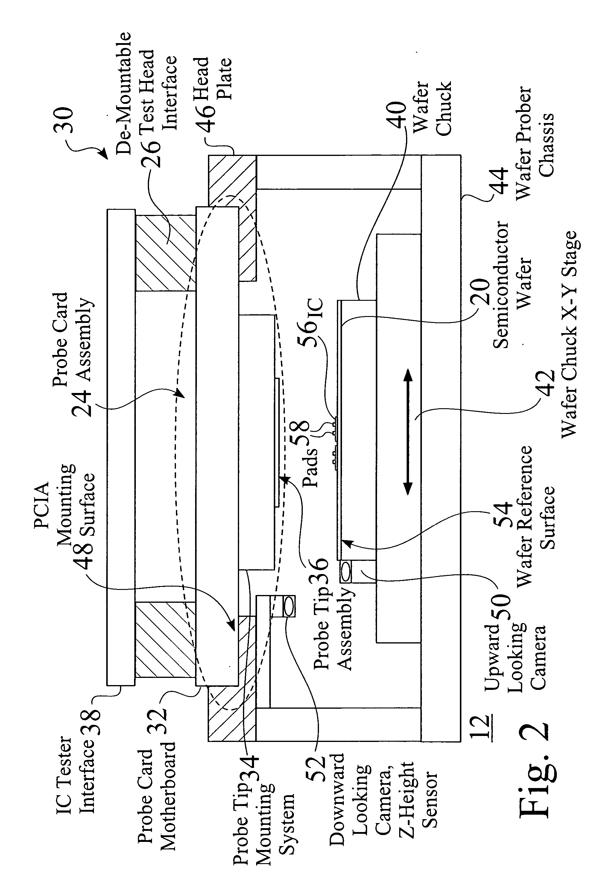
[0058] Introductory disclosure regarding structures, processes and systems disclosed herein is seen in: U.S. Provisional Application No. 60 / 136,636 (NNEX0001PR), entitled Wafer Interface for High Density Probe Card, filed May 27, 1999; U.S. Provisional Application No. 60 / 146,241 (NNEX0003PR), entitled Method of Massively Parallel Testing of Circuits, filed Jul. 28, 1999; U.S. Provisional Application No. 60 / 573,541 (NNEX0019PR), entitled Quick-Change Probe Chip, filed May 20, 2004; U.S. Provisional Application No. 60 / 592,908 (NNEX0021PR), entitled Probe Card Assembly with Rapid Fabrication Cycle, filed Jul. 29, 2004; U.S. Provisional Application No. 60 / 651,294 (NNEX0015PR), entitled Nano-Contactor Embodiments for IC Packages and Interconnect Components, filed Feb. 8, 2005; U.S. patent application Ser. No. 10 / 870,095 (NNEX0001CIP2), entitled Enhanced Compliant Probe Card Systems Having Improved Planarity, US Filing Date Jun. 16, 2004; U.S. patent application Ser. No. 10 / 178,103 (NNEX0...


PUM

PropertyMeasurementUnit
thickaaaaaaaaaa
thicknessaaaaaaaaaa
thicknessaaaaaaaaaa

Abstract

An improved interconnection system and method is described, such as for connectors, socket assemblies and / or probe card systems. An exemplary system comprises a probe card interface assembly (PCIA) for establishing electrical connections to a semiconductor wafer mounted in a prober. The PCIA comprises a motherboard parallel to the semiconductor wafer having an upper surface and an opposing lower planar mounting surface, a reference plane defined by a least three points located between the lower surface of the motherboard and the wafer, at least one component located below the motherboard mounting surface, and a mechanism for adjusting the planarity of the reference plane with respect to the wafer. A probe chip having a plurality of spring probes extending there from is mountable and demountable from the PCIA, without the need for further planarity adjustment. The interconnection structures and methods preferably provide improved fabrication cycles.

Description

CROSS REFERENCE TO RELATED APPLICATIONS [0001] This Application claims priority to (NNEX0019PR) U.S. Provisional Application No. 60 / 573,541, entitled Quick-Change Probe Chip, filed May 20, 2004; (NNEX0021PR) U.S. Provisional Application No. 60 / 592,908, entitled Probe Card Assembly with Rapid Fabrication Cycle, filed Jul. 29, 2004; and (NNEX0015PR) U.S. Provisional Application No. 60 / 651,294, entitled Nano-Contactor Embodiments for IC Packages and Interconnect Components, filed Feb. 8, 2005. [0002] This Application is also a Continuation In Part of U.S. patent application Ser. No. 10 / 870,095 (NNEX0001CIP2), entitled Enhanced Compliant Probe Card Systems Having Improved Planarity, US Filing Date Jun. 16, 2004, which is a Continuation-In-Part of U.S. patent application Ser. No. 10 / 178,103 (NNEX0001CIP), entitled Construction Structures and Manufacturing Processes for Probe Card Assemblies and Packages Having Wafer Level Springs, US Filing Date Jun. 24, 2002, which is a Continuation-In-...

Claims


Application Information

Patent Timeline
Patent Type & Authority Applications(United States)
IPC IPC(8): G01R1/073G01R31/02G01R31/28H05K7/06
CPCG01R1/07378Y10T29/49222Y10T29/49117G01R31/2889G01R1/06G01R31/26H01L22/00G01R1/073
Inventor CHONG, FU CHIUNGKAO, ANDREWMCKAY, DOUGLASLITZA, ANNAMODLIN, DOUGLASMOK, SAMMYPAREKH, NITINSWIATOWIEC, FRANK JOHNSHAN, ZHAOHUI
Owner ADVANTEST SINGAPORE PTE LTD
Why Eureka
Try Eureka