
Metallic material for electric or electronic parts

Inactive Publication Date: 2005-12-22
FURUKAWA ELECTRIC CO LTD
View PDF13 Cites 18 Cited by
  • Summary
  • Abstract
  • Description
  • Claims
  • Application Information

AI Technical Summary

Benefits of technology

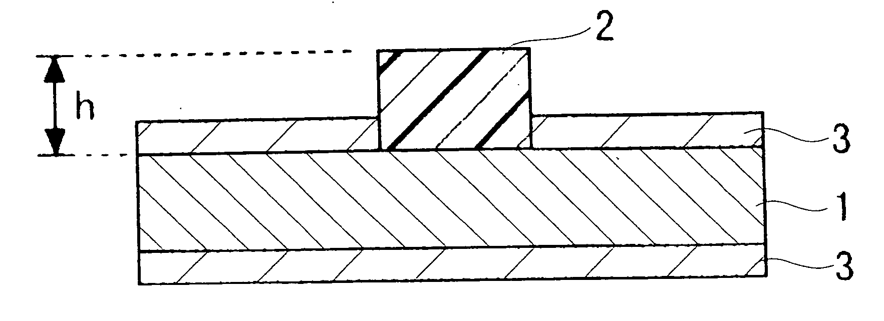
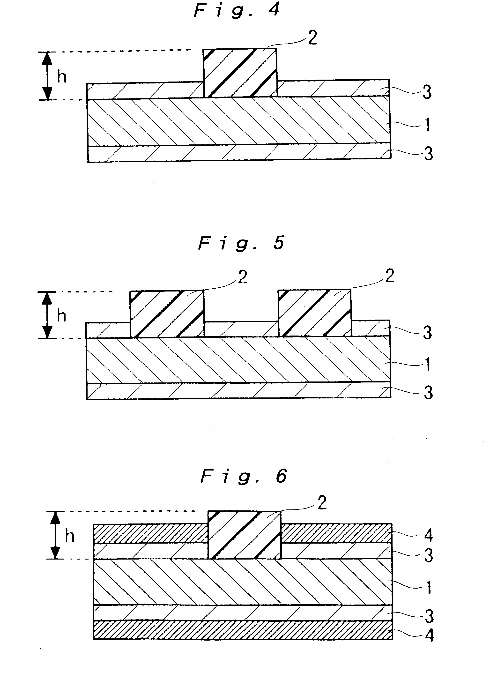
[0042] The metallic layer(s) may be formed into the form of a single layer or plural layers. For example, in the case of a use which is to be subjected to solder connecting, the thickness of the outermost metallic layer out of the above-mentioned metallic layers is preferably made into 1 μm or more, which causes the wettability to a solder to be satisfactorily kept and makes melt-connecting, such as reflow solder connecting, possible. The upper limit thereof is about 20 μm. Even if the thickness is made more than the limit, the advantageous effects are saturated. In uses other than it, the thickness of the outermost metallic layer is preferably from 0.1 to 10 μm in view of corrosion resistance, resin adhesion property or the like. With respect to the metallic layers other than the outermost layer also, the thickness thereof preferably ranges from 0.1 to 10 μm.
[0043] In the case of the plural layers, the number of the layers is more preferably 2 from the viewpoint of cost performance. The thickness of each of the layers of the multi-layered structure is preferably from 0.1 to 10 μm.
[0044] The material of the metallic layer(s) formed on the metallic substrate is decided depending on the material of the metallic substrate, the kind and use of a material-used part, required characteristics, allowable costs, and the like. In all cases, however, a metal satisfying the basic necessary characteristics required in the present invention is selected. In the metallic layer(s), there can be generally used at least one metal from Ni, Cu, Sn, Ag, Pd and Au, or an alloy, eutectic material or compound comprising at least one of the above-mentioned metals.
[0045] In view of cost performance, in the case of the single layer film, it is preferred to use any series (metal, alloy, eutectic material or compound) of Ni, Sn or Ag. In the case of the plural-layered film, it is preferred to use any series of Ni or Cu in the inner layer side (undercoat) and use any series of Sn, Ag, Pd or Au in the outer layer side. In the case that the metallic layers are three or more layers, it is preferred to use any series of Cu, Ag or Pd in the intermediate layer(s).
[0046] An alloy can be used in the Ni-series or Cu-series undercoat layer also. It is sufficient that the structure thereof is made of a simple substance or a simple-substance plural-layer. If the thickness is too small, many pinholes are generated. If the thickness is too large, cracks are easily generated at the time of processing. Accordingly, the thickness is preferably from about 0.1 to 2 μm.
[0047] A structure wherein its undercoat is made into one or more films of any series of Ni or Cu and its outer layer is made into a Sn-series film is widely used since the structure satisfies general necessary characteristics and is economical.

Problems solved by technology

However, the above-mentioned metallic casing or the like have the drawback that the internal volume thereof becomes smaller as the height thereof becomes smaller, and consequently, an insulating property cannot be sufficiently ensured between the electric or electronic part, such as a case, cover, cap, or casing (a case with a cover), and parts built therein.
However, the method has the problem that costs increase, and the production process is also complicated.

Method used


Image

  • Metallic material for electric or electronic parts
  • Metallic material for electric or electronic parts
  • Metallic material for electric or electronic parts

Examples


example 1

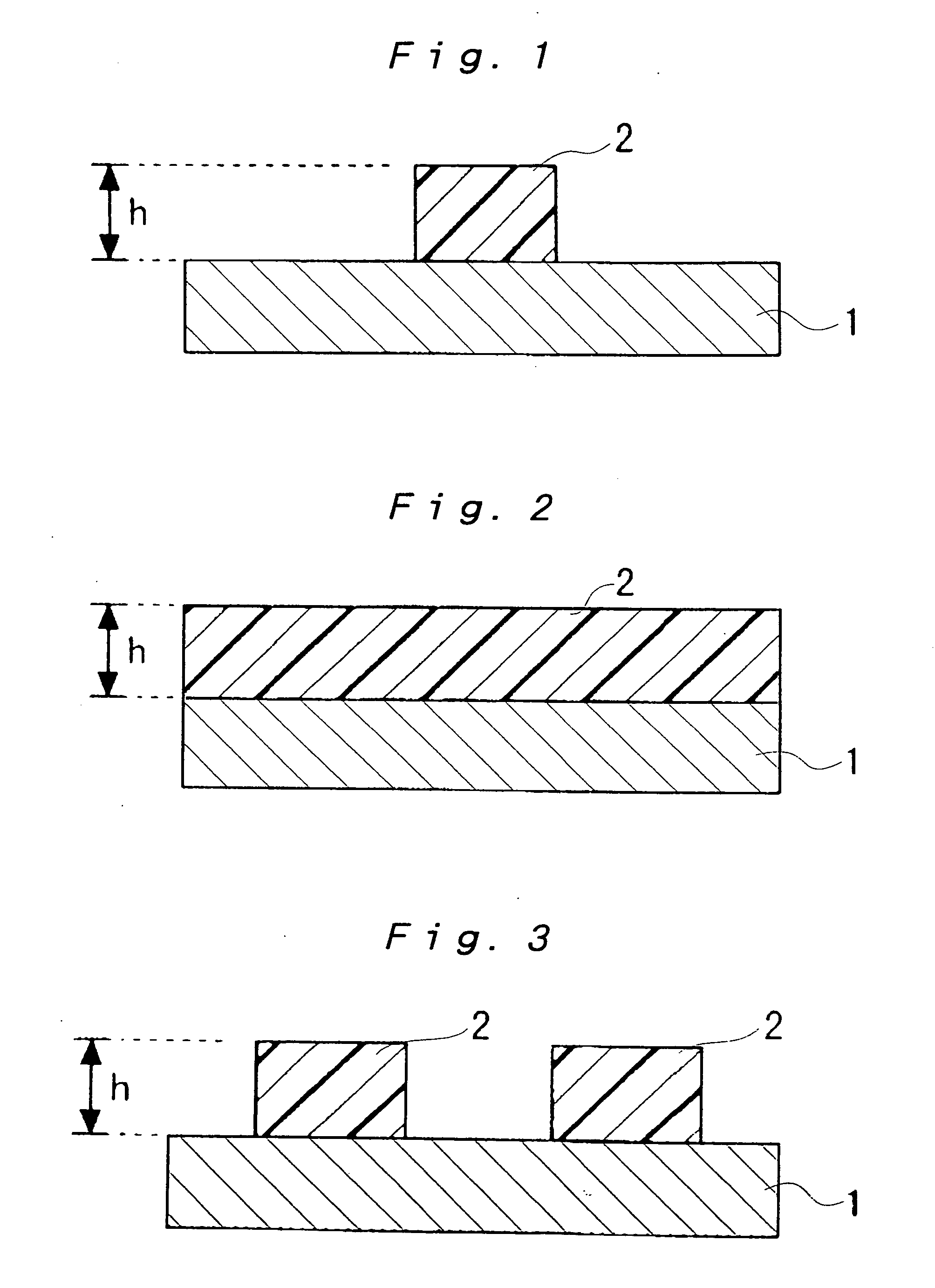
[0078] A Cu-6% by mass Sn-0.2% by mass P alloy (phosphorus bronze, a JIS alloy number C7521 (nickel silver), and an Fe-42% by mass Ni alloy (42 alloy) were each melted and cast to prepare an ingot. The ingot was subjected to hot rolling followed by cold rolling to prepare strips having 0.1 mm thick and 20 mm wide. Each of the strips was subjected to respective steps of electrolytic degreasing, acid-washing treatment, water-washing, and drying in this order. Before the drying step, a part of the strips were dipped into a solution wherein an epoxy-series silane coupling agent was dissolved in water, thereby subjecting the strips to silane coupling treatment.

[0079] Next, a heat-resistant resin film having a thickness of 3 μm or more was formed on each of the dried strips and in a place where insulation was required by either of the following method (a) or method (b), to thereby manufacture samples Nos. 1 to 27.

[0080] (a) A varnish made of a polyimide solution or precursor solution or...

example 2

[0086] A strip material (sample No. 28) was manufactured in the same manner as the samples Nos. 8 to 20 in Example 1 except that no metallic layer was formed, and the same tests as in Example 1 were conducted. The test results and the construction of the strip material are shown in Table 1.

example 3

[0087] A strip material (sample No. 29) was manufactured in the same manner as the sample No. 1 in Example 1 except that the thickness of the heat-resistant resin film was set to 2 μm, and the same tests as in Example 1 were conducted. The test results and the construction of the strip material are shown in Table 1.


PUM

PropertyMeasurementUnit
Heightaaaaaaaaaa
Metallic bondaaaaaaaaaa

Abstract

A metallic material for electric or electronic parts containing a resin film on or over at least a part of a metallic substrate; and an electric or electronic part using the metallic material.

Description

TECHNICAL FIELD [0001] The present invention relates to a metallic material suitable for electric or electronic parts (casings, cases, covers, caps or the like), such as low profile casings comprising therein elements mounted on a printed board or the like of electric or electronic machinery and tools, in particular, a portable equipment or the like. BACKGROUND ART [0002] An individual part that is to be mounted on a printed board or the like of electric or electronic machinery and tools, such as a ceramic oscillator, a quartz oscillator, a voltage-controlled oscillator, an SAW filter, a diplexer, a coupler, a balun, an LPF, a BPF, or a dielectric duplexer; and various module parts each comprising therein plurality of the above-mentioned elements (such as an antenna switch module, a front end module, an RF-integrated module, a bluetooth module, an image sensor module, and a tuner module), as well as detecting switches or other parts, are each used by being put into a metallic casing...

Claims


Application Information

Patent Timeline
IPC IPC(8): H01L23/14H05K9/00
CPCH01L23/142Y10T428/24917H05K9/0084H01L2924/0002H01L2924/00C23C26/00H01L23/02H05K5/00
Inventor TANI, TOSHIOSUZUKI, SATOSHIMESAKI, MASAKAZU
Owner FURUKAWA ELECTRIC CO LTD
Learn More