Image sensor module structure comprising wire bonding package and method of manufacturing the image sensor module structure

a technology of image sensor and wire bonding package, which is applied in the direction of radio frequency control devices, instruments, television systems, etc., can solve the problems of difficult to reduce the size of the image sensor module structure, damage to the wires b>116/b>, and horizontal size, so as to reduce the horizontal size

Inactive Publication Date: 2005-12-29
SAMSUNG ELECTRONICS CO LTD
View PDF15 Cites 65 Cited by
  • Summary
  • Abstract
  • Description
  • Claims
  • Application Information

AI Technical Summary

Benefits of technology

[0015] Embodiments of the present invention provide an image sensor module structure with a reduced horizontal size, which is suitable for a compact mobile camera system, and a method of manufacturing the image sensor module structure.
[0016] Embodiments of the present invention also provide an image sensor module structure, which can reduce a possibility of misalignment during a process of attaching a housing on a substrate and prevent damage to wires due to misalignment, and a method of manufacturing the image sensor module structure.
[0017] Embodiments of the present invention also provide an image sensor module structure, which can reduce difficulty in sealing contact portions and can be easily manufactured using typical semiconductor manufacturing technology, and a method of manufacturing the image sensor module structure.
[0018] An image sensor module structure according to the present invention attaches a filter projecting downwardly from a housing body on an image sensor chip, so that a housing can be attached on an image sensor package without attaching the housing body on a substrate. The image sensor package is a wire bonding package where wires are interposed between the substrate and the housing body. An underfiller is filled between the substrate and the housing body using an underfill process to prevent the wires from being damaged and impurities from entering a light receiving area. However, in the image sensor module structure according to the present invention, the housing particularly, a lens assembly can have various structures and the lens assembly can be inserted and attached to the housing body in various ways.

Problems solved by technology

The areas d1 and d2 result in an increase of a horizontal size of the image sensor module structure 100, thereby making it difficult to reduce the size of the image sensor module structure 100.
Consequently, if slight misalignment occurs during a process of attaching the housing body 120, the wires 116 may be damaged.
This vacuum process makes the manufacturing process more cumbersome.
In addition, contact portions between the lower sidewall 120c and the substrate 110 and between the middle sidewall 120b and the filter 130 must be sealed elaborately, thereby making the manufacturing process more difficult.

Method used


Image

  • Image sensor module structure comprising wire bonding package and method of manufacturing the image sensor module structure
  • Image sensor module structure comprising wire bonding package and method of manufacturing the image sensor module structure
  • Image sensor module structure comprising wire bonding package and method of manufacturing the image sensor module structure

Examples


Embodiment Construction

[0029] The present invention will now be described more fully with reference to the accompanying drawings, in which preferred embodiments of the invention are shown. The thickness of layers and / or the size of areas are exaggerated for clarity in the drawings. Like reference numerals refer to like elements throughout.

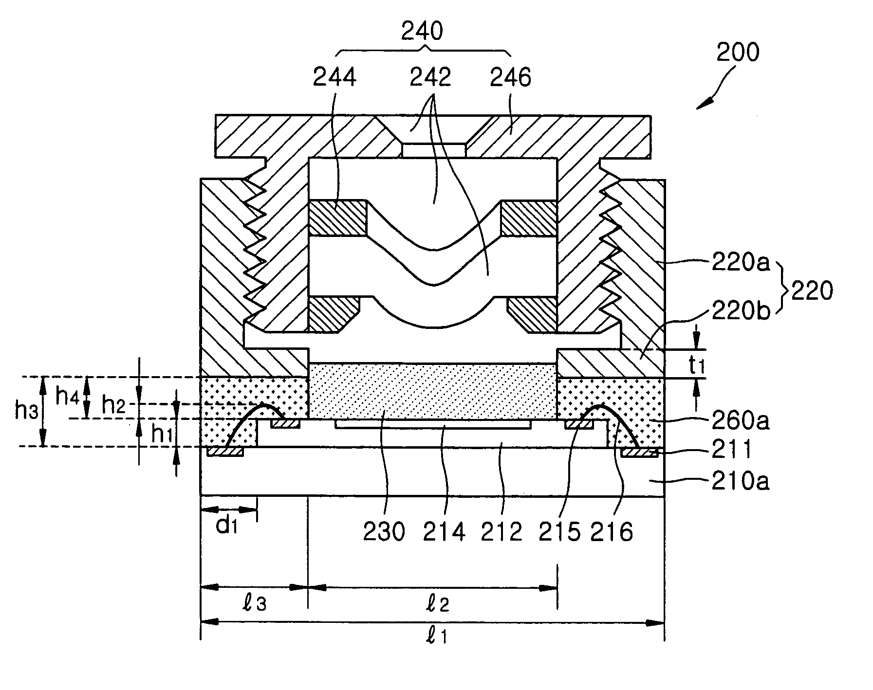
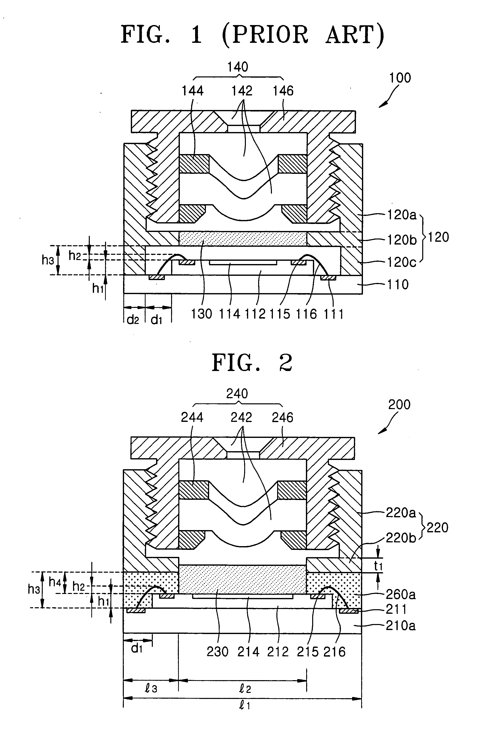
[0030]FIG. 2 is a schematic sectional view of an image sensor module structure 200 according to an exemplary embodiment of the present invention.

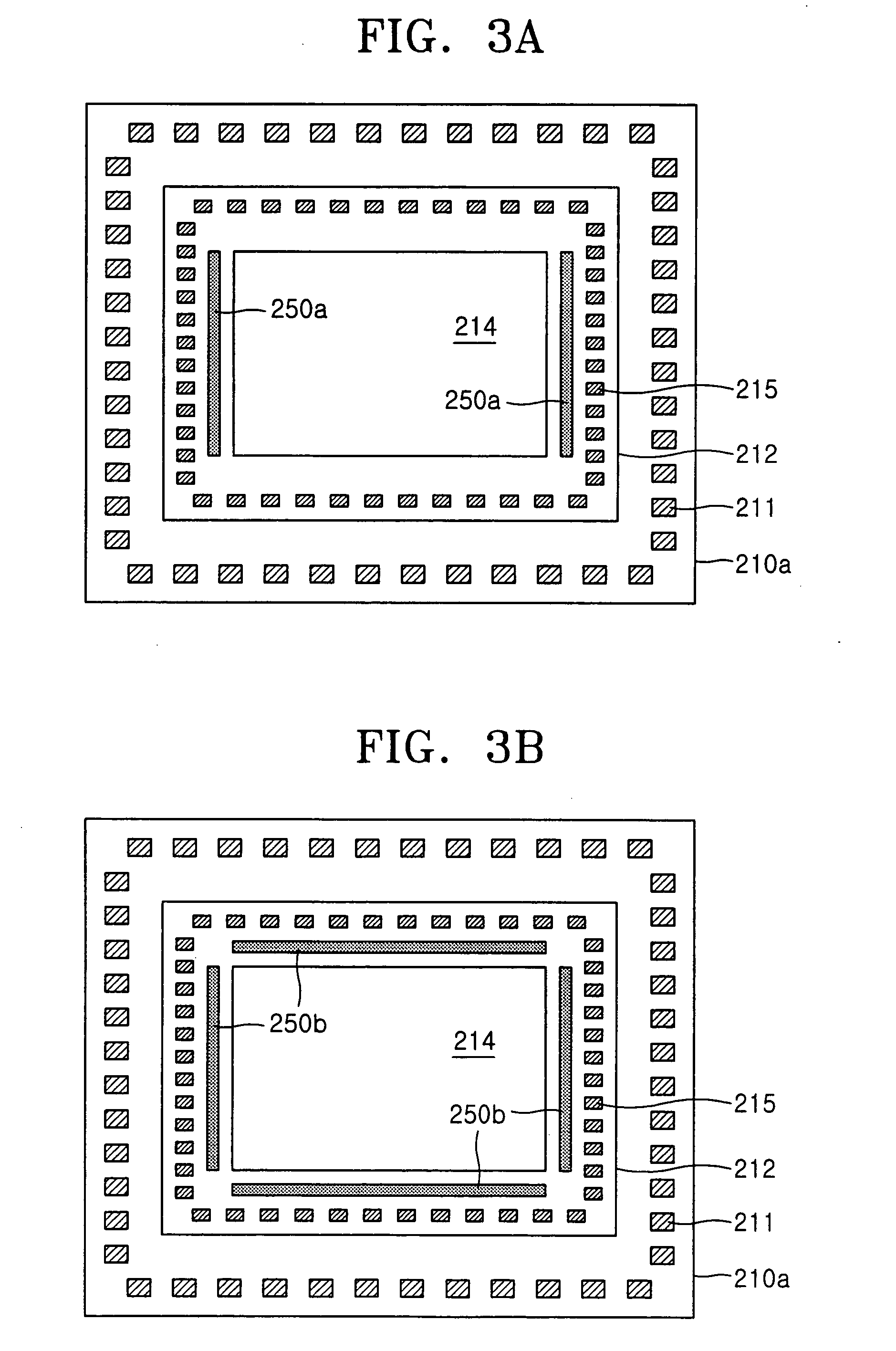
[0031] Referring to FIG. 2, the image sensor module structure 200 includes an image sensor package composed of a substrate 210a, an image sensor chip 212, and wires 216, a housing body 220, a filter 230, a lens assembly 240, and an underfiller 260a. The housing body 220, the filter 230, and the lens assembly 240 are collectively referred to as a housing. The filter may be an optical filter, an infrared filter, an ultraviolet filter, or any combination thereof.

[0032] The image sensor package is a wire bonding type, and include...


PUM


Abstract

An image sensor module structure includes an image sensor package, a housing, and an underfiller. The image sensor package includes a substrate having interconnection pads formed on an outermost edge. The housing includes a filter projecting from a bottom surface of a housing body. The projecting filter is attached on an image sensor chip using various adhesive patterns. Further, the underfiller is formed in a space between the housing body and the image sensor package.

Description

BACKGROUND OF THE INVENTION [0001] This application claims the priority of Korean Patent Application No. 2004-49727, filed on Jun. 29, 2004, in the Korean Intellectual Property Office, the disclosure of which is incorporated herein in its entirety by reference. [0002] 1. Field of the Invention [0003] The present invention relates to an image sensor module structure and a method of manufacturing the image sensor module structure, and more particularly, to an image sensor module structure comprising a wire bonding package, and a method of manufacturing the image sensor module structure. [0004] 2. Description of the Related Art [0005] Image sensors are semiconductor electronic devices that convert optical information into electrical signals. Examples of Image sensors include charge coupled device (CCD) image sensors and complementary metal oxide semiconductor (CMOS) image sensors. As cameras, camcorders, personal computer (PC) cameras, and surveillance cameras are digitalized, applicat...

Claims


Application Information

Patent Timeline
Patent Type & Authority Applications(United States)
IPC IPC(8): H01L27/00H01L27/146
CPCH01L27/14618H01L2924/0002H01L2924/00H01L27/14H01L23/12H01L27/146H01L21/60
Inventor KONG, YUNG-CHEOLSEO, BYOUNG-RIMDO, JAE-CHEON
Owner SAMSUNG ELECTRONICS CO LTD
Why Eureka
Try Eureka