Nitride based semiconductor device

Active Publication Date: 2005-12-29
SAMSUNG ELECTRONICS CO LTD
View PDF5 Cites 15 Cited by
  • Summary
  • Abstract
  • Description
  • Claims
  • Application Information

AI Technical Summary

Benefits of technology

[0010] Therefore, the present invention has been made in view of the above problems, and it is an object of the present invention to provide a nitride semiconductor device having a novel lower clad layer for improving internal quantum efficiency, capable of increasing efficiency of carrier injected to an active layer while overcoming a problem associated with reduction of light efficiency due to the occurrence of stress.

Problems solved by technology

As a result, this phenomenon causes a reduction of light efficiency of the device.

Method used


Image

  • Nitride based semiconductor device
  • Nitride based semiconductor device
  • Nitride based semiconductor device

Examples


Embodiment Construction

[0026] Now, the present invention will be described in detail with reference to the attached drawings.

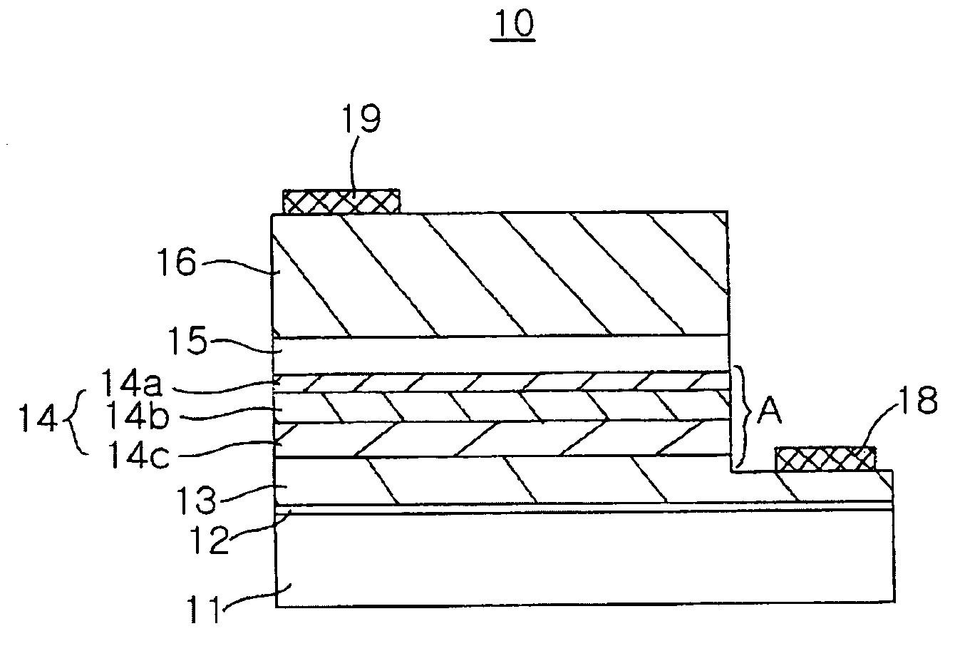
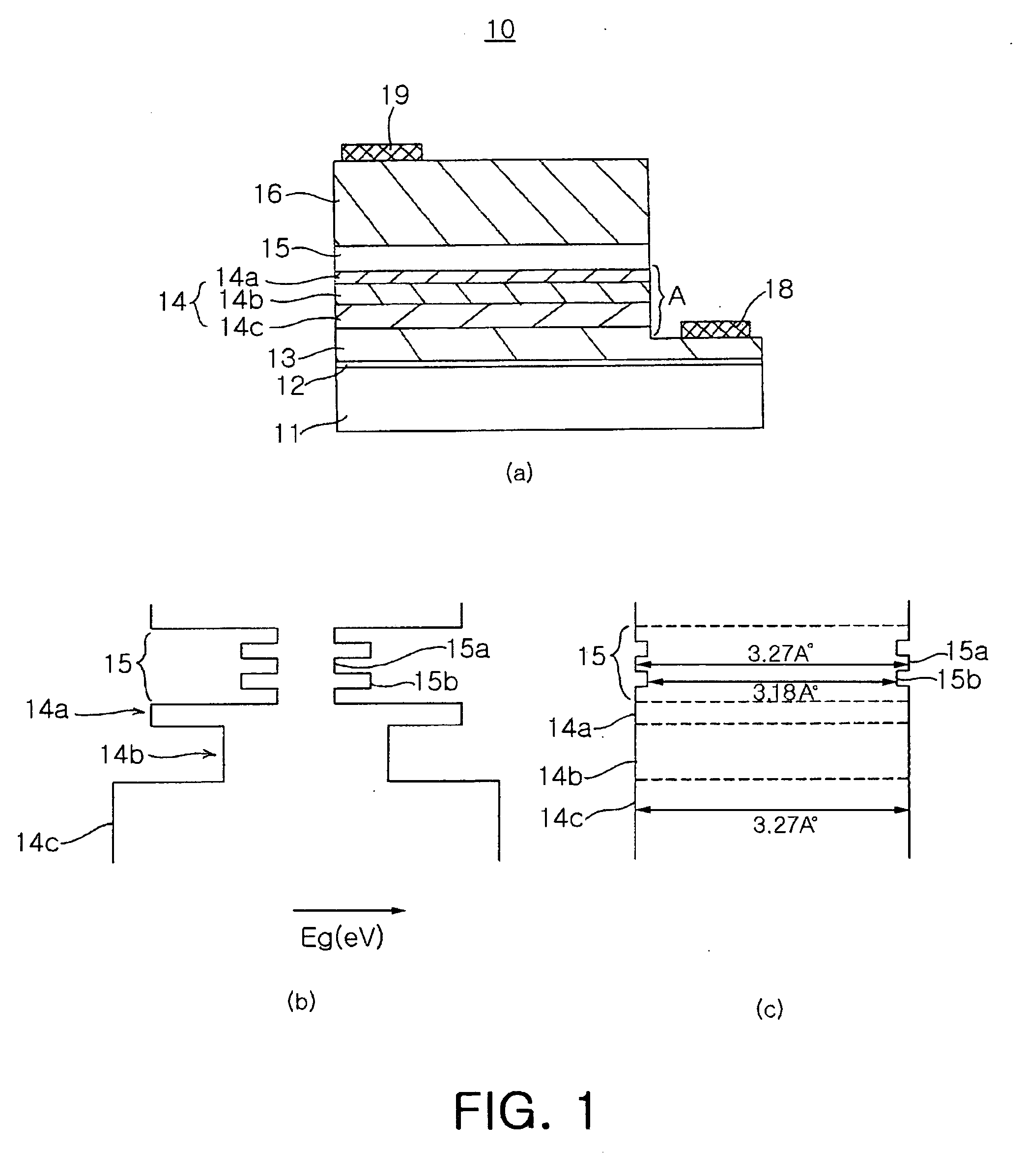
[0027]FIG. 1a is a cross-sectional side view of a nitride semiconductor device 10 in accordance with one embodiment of the present invention.

[0028] Referring to FIG. 1a, the nitride semiconductor device 10 includes a nitride semiconductor laminate structure on a substrate 11 having a buffer layer 12 formed thereon. The substrate 11 may be sapphire, SiC or GaN. The buffer layer 12 is a low temperature nucleus-growth layer made of AlxGa1−xN.

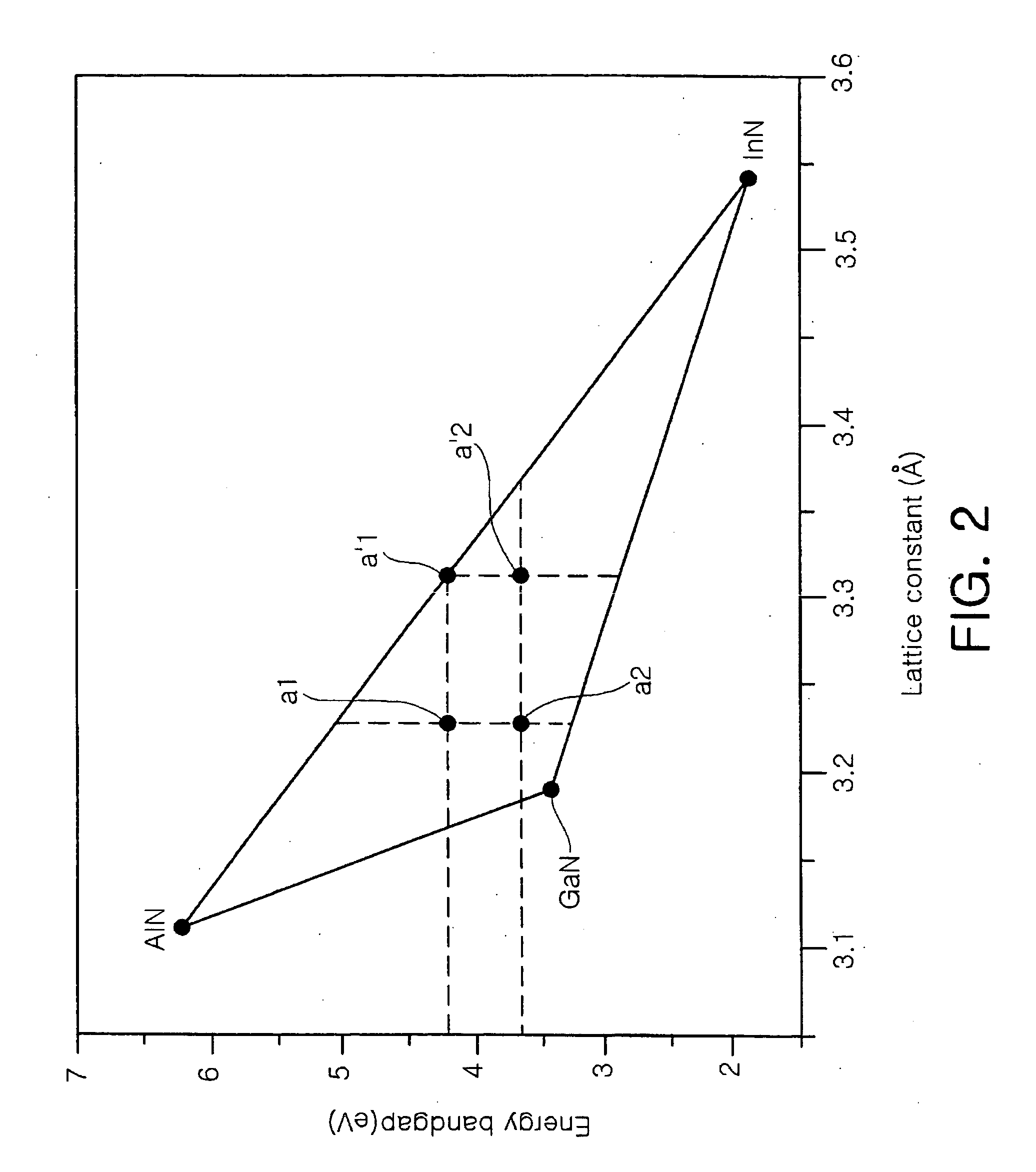
[0029] The nitride semiconductor laminate structure may include an n-type GaN layer 13, an n-type clad layer 14, an active layer 15 and a p-type clad layer 16 sequentially formed on the buffer layer 12. The n-type clad layer 14 in accordance with the present invention is made of quaternary InAlGaN, and in order to increase electron injection efficiency, is composed of a first, second and third nitride semiconductor layers 14a, 14b and 14c, seque...


PUM


Abstract

The present invention provides a nitride semiconductor device comprising an active layer of a quantum well structure, a first conductive clad layer and a second conductive clad layer. The first conductive clad layer is made of the quaternary nitride semiconductor InAlGaN having a lattice constant equal to or larger than that of the active layer and includes a first nitride semiconductor layer having an energy band gap larger than that of the active layer, a second nitride semiconductor layer having an energy band gap smaller than that of the first nitride semiconductor layer and a third nitride semiconductor layer having an energy band gap larger than that of the second nitride semiconductor layer, sequentially closer to the active layer.

Description

BACKGROUND OF THE INVENTION [0001] 2. Field of the Invention [0002] The present invention relates to a nitride semiconductor device such as a light-emitting device, laser, or the like, and more particularly to a nitride semiconductor device capable of increasing carrier injection efficiency and at the same time, capable of preventing reduction of light efficiency due to stress by improving a structure of a lower clad layer of an active layer thereof. [0003] 2. Description of the Related Art [0004] Generally, a nitride semiconductor device is a high output power optical device that produces short wavelength light such as blue light, green light, or the like, thus enabling it to produce a variety of colors, and is actively employed as a light emitting diode (LED) and a laser diode (LD). Usually, the nitride semiconductor device is prepared by growing an epitaxial layer on a substrate such as sapphire or SiC using Metal Organic Chemical Vapor Deposition (MOCVD), and the like. [0005] Li...

Claims


Application Information

Patent Timeline
IPC IPC(8): H01L29/22H01L33/02H01L33/06H01L33/32
CPCB82Y20/00H01L33/32H01L33/06H01L33/02
Inventor KIM, SUN WOOOH, JEONG TAKKIM, JE WON
Owner SAMSUNG ELECTRONICS CO LTD
Why Eureka
Try Eureka