Power transistor device and a power control system for using it

a power transistor and power control technology, applied in the direction of electronic switching, emergency protective arrangements for limiting excess voltage/current, pulse techniques, etc., can solve the problems of increasing the cost of the chip, reducing the breaking strength of an abnormality such as the earth fault of the power supply, and increasing the size of the chip. the effect of reliability

Inactive Publication Date: 2005-12-29
FUJIKI ATSUSHI +1
View PDF9 Cites 41 Cited by
  • Summary
  • Abstract
  • Description
  • Claims
  • Application Information

AI Technical Summary

Benefits of technology

[0005] As heavy-current flows into a power MOS transistor, it is important so as to reduce loss in the transistor to reduce the ON-state resistance. Then, these inventors discussed a power transistor in which the length of a channel for distance between a source and a drain was relatively extended so as to reduce the ON-state resistance by configuring structure (hereinafter called trench structure) where a groove was made over a semiconductor substrate and a gate electrode made of polysilicon or others was formed by filling it in the groove in the vertical type power MOS transistor provided with a source electrode on one side and a drain electrode on the other side.
[0010] The object of the invention is to provide technique for protecting from overcurrent a power MOS transistor using a transistor having trench structure and enabling the enhancement of the reliability.
[0011] Another object of the invention is to provide the overcurrent protection technique of a power MOS transistor excellent in a response characteristic until the current of the power transistor is reduced since overcurrent is detected for enabling minimizing the extension of chip size and the increase of the cost.
[0015] According to the above-mentioned means, as the current of the power MOS transistor is inhibited by the built-in protection circuit before the current of the power MOS transistor is cut off by the external control circuit when current equal to or exceeding a predetermined value flows in the power MOS transistor, the destruction of the power MOS transistor can be avoided even if overcurrent flows into the power MOS transistor by the short-circuit of a load or others.
[0018] That is, according to the invention, the power MOS transistor using a transistor having trench structure is protected from overcurrent and the reliability can be enhanced.

Problems solved by technology

As a result, the transistor having trench structure can realize lower ON-state resistance, compared with a transistor having normal planar structure, however, the transistor having trench structure has a tendency that as the mutual conductance (gm) is large and the saturated drain current is also much, the breaking strength in an abnormality such as the earth fault of power supply decreases.
A method of accelerating the speed of a response by providing a control circuit for controlling a power transistor in the same semiconductor chip as the power transistor is conceivable, however, as a result, a problem that the size of the chip is extended and the cost of the chip is increased occurs.
Particularly, as coupling between devices is difficult when a vertical type transistor is also used for a transistor for configuring the control circuit in case the power transistor has trench structure, a transistor of a horizontal type is required to be used.
However, as desired characteristics cannot be acquired when the MOS transistor of a horizontal type is formed in a process for the vertical type transistor, a problem that the number of processes is required to be increased and thereby, the cost of the chip is further increased occurs.

Method used


Image

  • Power transistor device and a power control system for using it
  • Power transistor device and a power control system for using it
  • Power transistor device and a power control system for using it

Examples


Embodiment Construction

[0025] Referring to the drawings, a preferred embodiment of the invention will be described below.

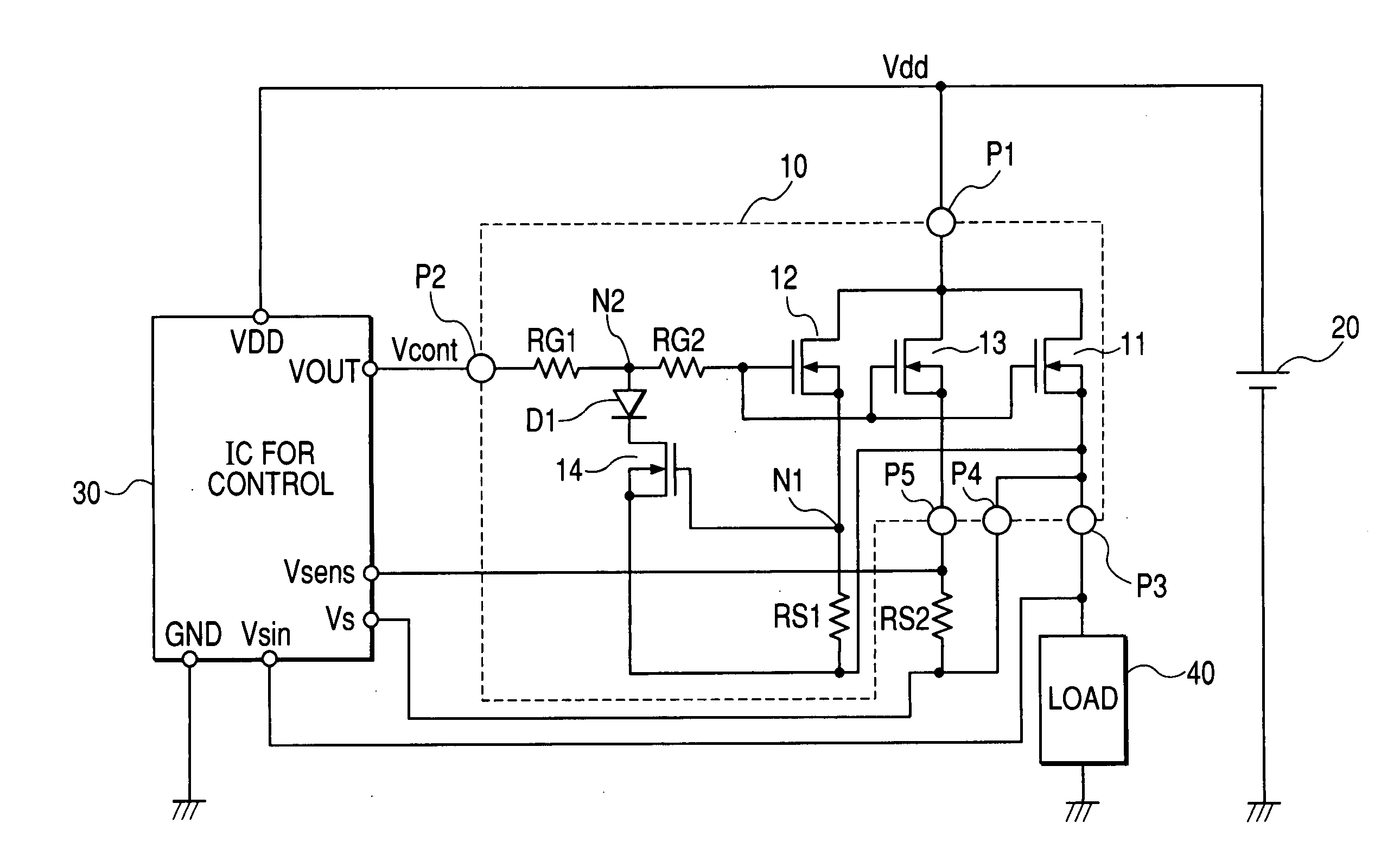
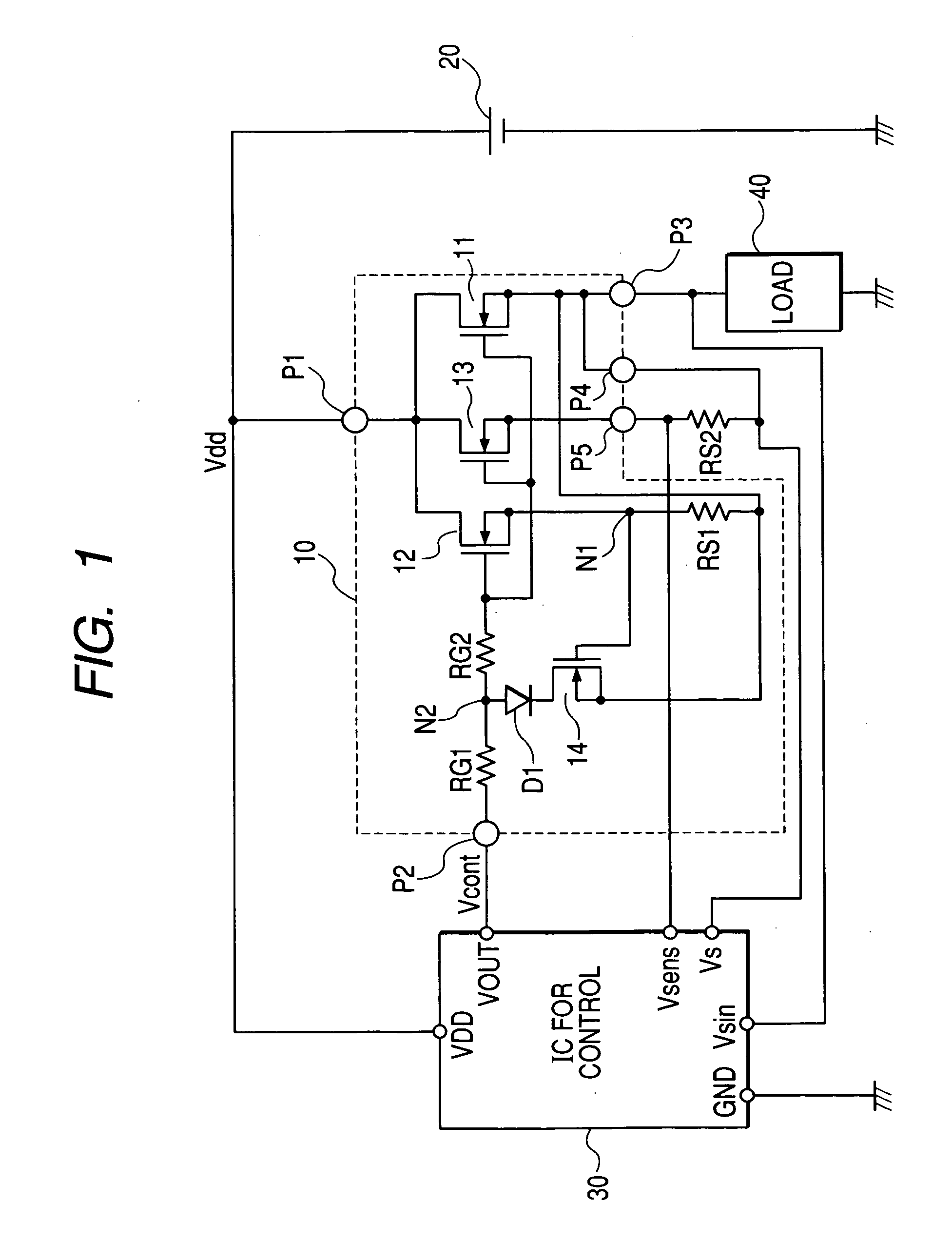
[0026]FIG. 1 shows an embodiment of a power MOS transistor device according to the invention and a power control system to which the power MOS transistor device is applied. Though it is not particularly limited, each device provided in a part encircled by a broken line 10 is formed in one semiconductor chip made of monocrystalline silicon as a semiconductor integrated circuit by a well-known MOS manufacturing process. In this specification, a semiconductor integrated circuit 10 including a power MOS transistor is called power IC.

[0027] The power IC 10 equivalent to this embodiment includes: a power MOS transistor 11 in which a drain terminal is coupled to a power supply voltage terminal P1 to which power supply voltage Vdd supplied from a direct voltage source 20 such as a battery is applied, and control voltage Vcont from IC for control 30 is applied to the gate terminal; and transis...


PUM


Abstract

The object of the invention is to protect a power MOS transistor using a transistor having trench structure from overcurrent and to enhance the reliability. To achieve the object, a power MOS transistor, a transistor for detecting current for detecting the current of the power MOS transistor and generating a detection signal supplied to an external control circuit and devices configuring a protection circuit for detecting the current of the power MOS transistor and inhibiting current by forcedly dropping the gate voltage of the power MOS transistor when current equal to or exceeding a predetermined value flows are provided in the same semiconductor chip.

Description

CROSS-REFERENCE TO RELATED APPLICATION [0001] The present application claims priority from Japanese patent application No. 2004-184792 filed on Jun. 23, 2004, the contents of which are hereby incorporated by reference into this application. BACKGROUND OF THE INVENTION [0002] The present invention relates to effective technique in applying to a power transistor that makes heavy-current flow and further, a power transistor device configured by a semiconductor integrated circuit, particularly relates to effective technique in utilizing for power MOS transistor IC the ON-state resistance of which is small and which is provided with an overcurrent protection function. [0003] Relatively heavy-current is made to flow in an electrical part such as a lamp of an automobile, a coil of a regulator and others. Heretofore, a semiconductor device called a power transistor has been used for a device for making current flow in a load requiring heavy-current. Such a power transistor has two types of ...

Claims


Application Information

Patent Timeline
Patent Type & Authority Applications(United States)
IPC IPC(8): H01L27/02H01L29/423H01L29/78H02H3/00H03K17/082
CPCH01L27/0251H01L29/4238H01L29/7803H03K17/0822H01L29/7813H01L29/7815H01L29/7804
Inventor FUJIKI, ATSUSHINAKASU, MASATOSHI
Owner FUJIKI ATSUSHI
Why Eureka
Try Eureka