High-voltage tolerant input buffer circuit

a buffer circuit and input technology, applied in logic circuit coupling/interface arrangement, pulse technique, instruments, etc., can solve the problems of sub-micron technology devices that cannot tolerate high-voltage, devices may experience temporary or even permanent damage, and circuit design for standard protocols has become more challenging, so as to speed up the transition and reduce power dissipation

Active Publication Date: 2005-12-29
STMICROELECTRONICS PVT LTD
View PDF4 Cites 22 Cited by
  • Summary
  • Abstract
  • Description
  • Claims
  • Application Information

AI Technical Summary

Benefits of technology

[0017] The PMOS and NMOS transistors are small-sized tr...

Problems solved by technology

Also, circuit designing for standard protocols has become more challenging.
Sub-micron technology devices cannot tolerate high-voltage because of reliability issues.
One notable problem in interfacing low-voltage circuitry with high-voltage circuitry is that if the voltage applied to the low-voltage circuitry gets too high, some devices may experience temporary or even permanent damage.
The gate-oxide stress causes threshold voltage to fluctuate because of tunneling effect—moreover, device lifetime dete...

Method used


Image

  • High-voltage tolerant input buffer circuit
  • High-voltage tolerant input buffer circuit
  • High-voltage tolerant input buffer circuit

Examples


Embodiment Construction

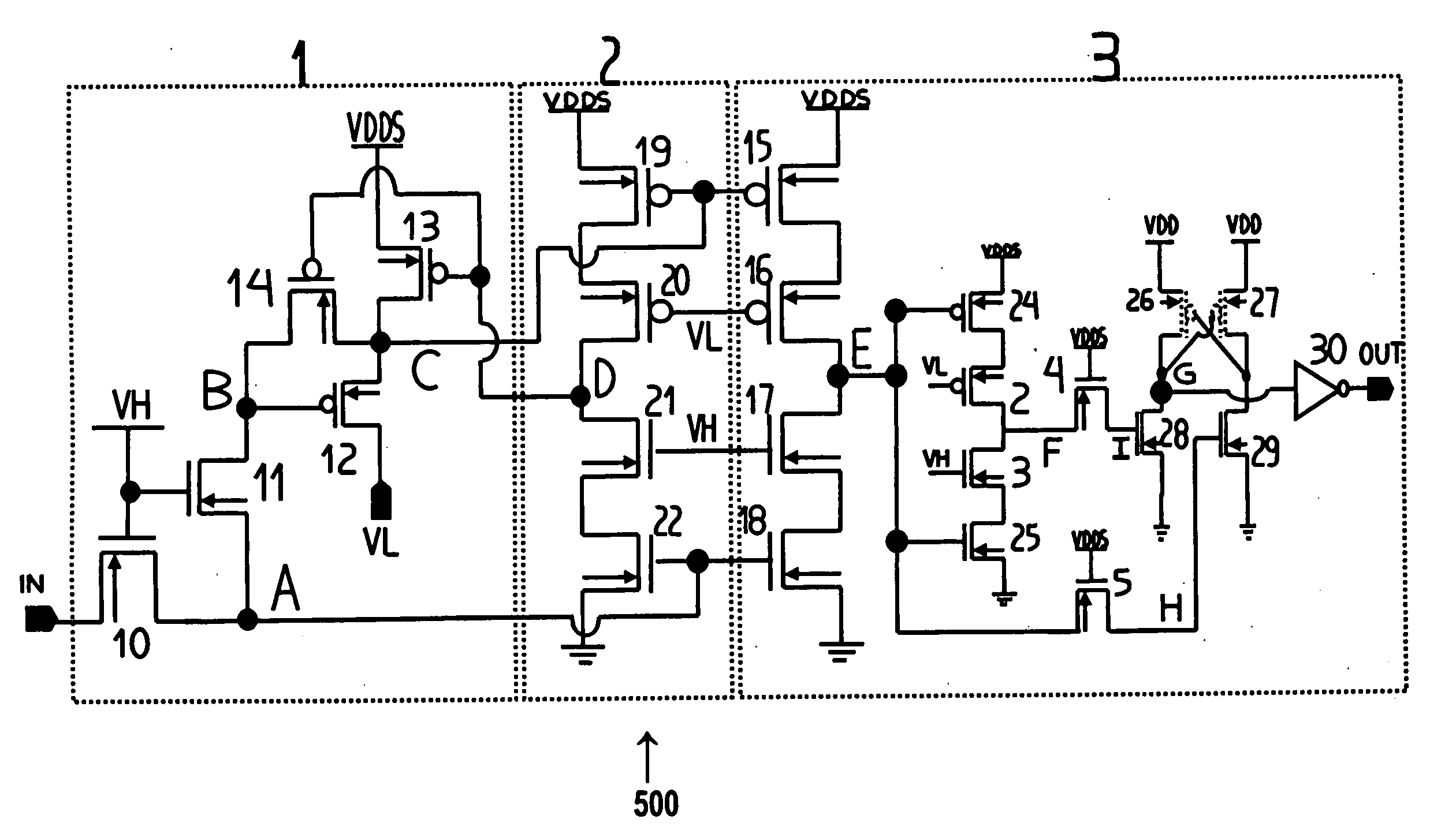
[0027] Two reference signals—one to protect PMOS and the other to protect NMOS—are used to avoid gate-oxide stress and Vds stress for oxide degradation and hot carrier effect respectively. Reference signals are necessary to be incorporated in the high-voltage designs with very short channel devices. So a single reference block can be used for the whole IO ring in the chip. Reference signals are shared among different IOs in the ring. For the sake of clear understanding of the new circuit, reference block has not been described.

[0028] In one embodiment (FIG. 6), the input buffer circuit includes an n-channel field effect transistor and a feedback circuitry to provide a safe voltage range for the input inverter. This feedback circuitry structure includes series transistors and two-reference signal and is responsive to the voltage applied at the output node. It is also responsible for pulling-up the voltage at the gate of p-channel MOS transistor in the input inverter for low power co...


PUM


Abstract

The present invention provides a high-voltage tolerant input buffer circuit including a first NMOS transistor having its source terminal connected to the input pin, its gate terminal connected to a first reference voltage and its drain terminal connected to a first output terminal; a second NMOS transistor having its gate terminal connected to said first reference voltage and its source terminal connected to said first output terminal; a first PMOS transistor having its gate terminal connected to the drain terminal of said second NMOS transistor, its drain terminal connected to a second reference voltage lower than said first reference voltage and its source terminal connected to a second output terminal; a second PMOS transistor having its drain terminal connected to the drain terminal of said second NMOS transistor, its source terminal connected to said second output terminal, and its gate terminal connected to a control voltage; and a third PMOS transistor having its drain terminal connected to said second output terminal, its source terminal connected to a supply voltage, and its gate terminal connected to said control voltage.

Description

RELATED APPLICATION [0001] The present invention claims priority of India Patent Application No. 1060 / Del / 2004, filed Jun. 8, 2004, which is incorporated herein in its entirety by this reference. FIELD OF THE INVENTION [0002] The present invention relates to an input buffer in the field of integrated circuits. Specifically, the invention pertains to a high-voltage tolerant input buffer circuit. BACKGROUND OF THE INVENTION [0003] With the advent of sub-micron technology, the device dimensions are decreased so as to be suitable in low cost and low power applications. Also, circuit designing for standard protocols has become more challenging. Sub-micron technology devices cannot tolerate high-voltage because of reliability issues. The gate-oxide breakdown voltage and / or the punch-through between source and drain typically define the voltage of a particular technology. To meet the standard protocols' electrical specifications, interface circuits must work at high voltages (e.g. 5V, 3.3 ...

Claims


Application Information

Patent Timeline
IPC IPC(8): G11C5/14H03K19/003H03K19/0185
CPCH03K19/018521H03K19/00315
Inventor GUPTA, SUSHIL KUMARGARG, PARAS
Owner STMICROELECTRONICS PVT LTD
Why Eureka
Try Eureka