Plasma processing method, plasma processing apparatus, and computer recording medium

Inactive Publication Date: 2005-12-29
TOKYO ELECTRON LTD
View PDF8 Cites 337 Cited by
  • Summary
  • Abstract
  • Description
  • Claims
  • Application Information

AI Technical Summary

Benefits of technology

[0019] According to the plasma processing apparatus structured as above, it is possible to perform t

Problems solved by technology

Thereby, it is possible to control the distribution of the nitrogen in the direction of the depth,

Method used


Image

  • Plasma processing method, plasma processing apparatus, and computer recording medium
  • Plasma processing method, plasma processing apparatus, and computer recording medium
  • Plasma processing method, plasma processing apparatus, and computer recording medium

Examples


embodiment 1

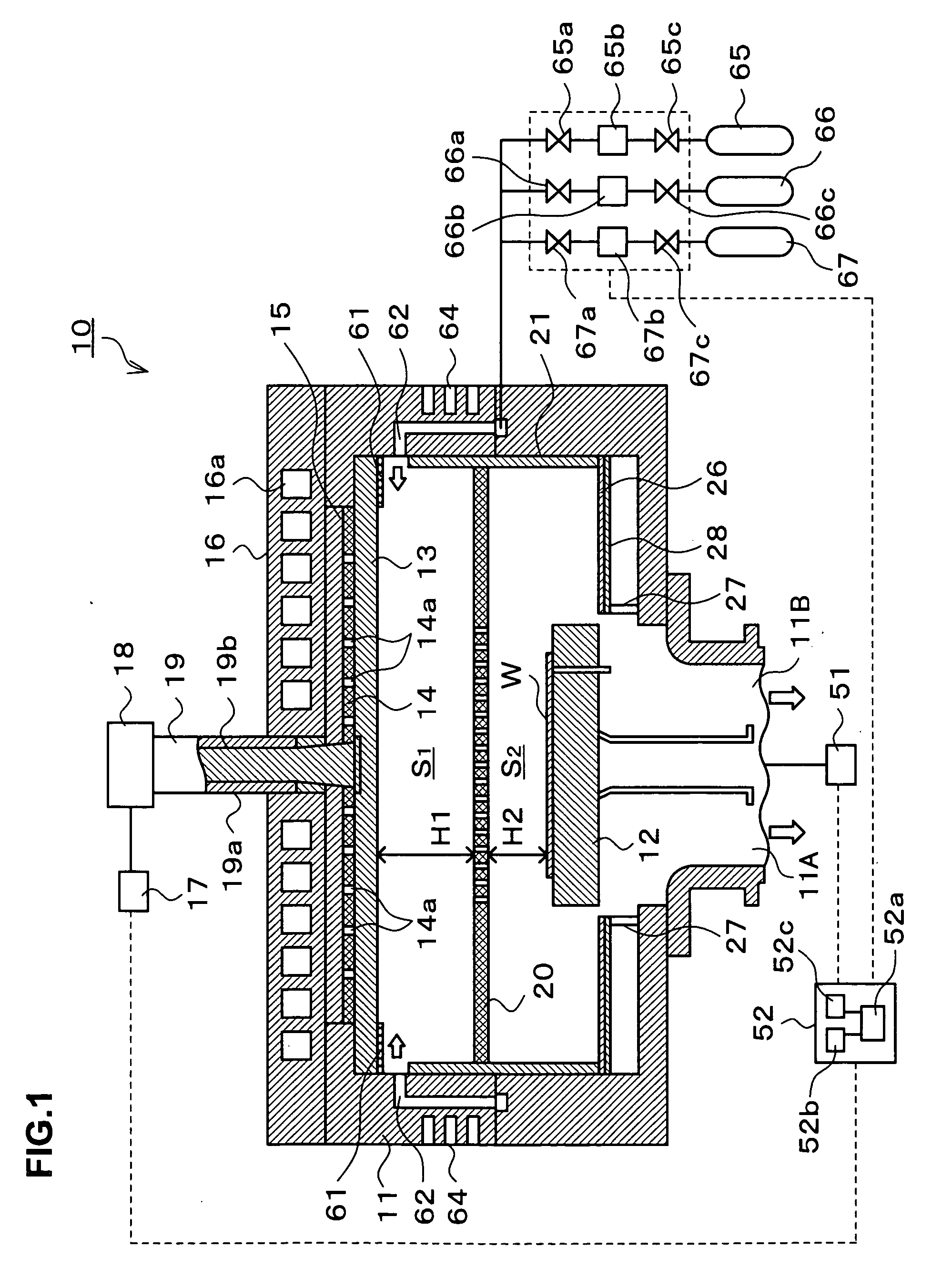
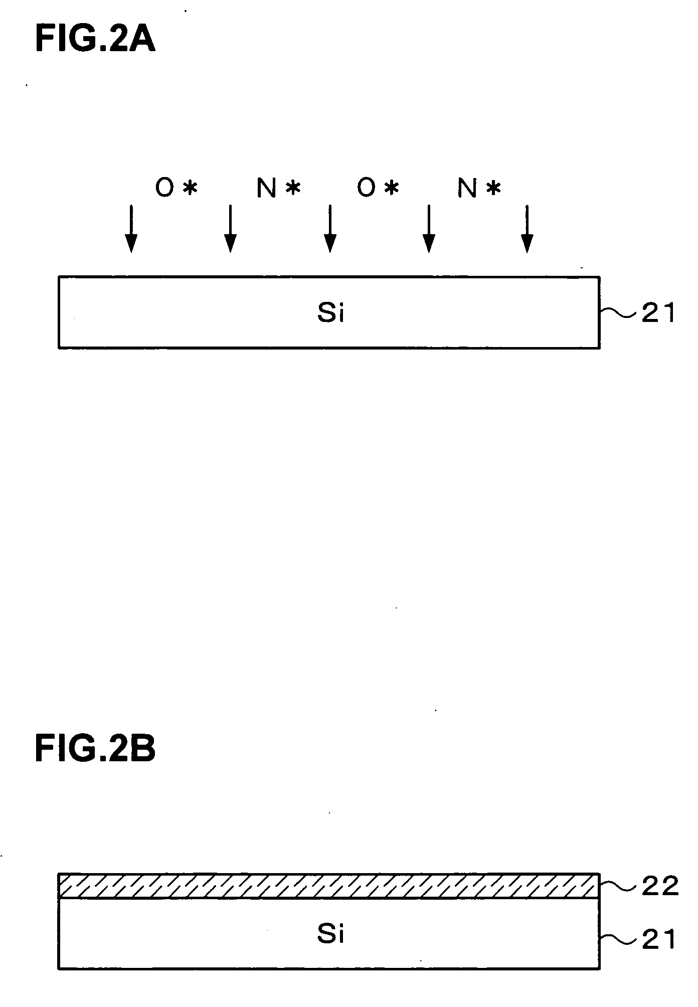
[0051] The oxygen radicals and the nitrogen radicals reaching the surface of a silicon substrate 21 subject the surface of the silicon substrate 21 to oxidation and nitridation processing as shown in FIG. 2B, to form a silicon oxynitride film 22 having a desired thickness (10 nm or less, for example). Thus, a semiconductor substrate having an insulating film formed by performing the oxidation and the nitridation at the same time (embodiment 1) is obtained.

[0052] Meanwhile, a semiconductor substrate having a thermal oxide film (conventional example); a semiconductor substrate having an insulating film which is subjected to plasma nitridation after plasma oxidation (comparative example 1); and a semiconductor substrate having a plasma oxidation film only (comparative example 2) are prepared for comparison purposes. Then, trap characteristics thereof, together with the aforesaid embodiment 1, are measured and compared for evaluation. The results are shown in FIGS. 4A, and 4B.

[0053] Th...

embodiment 2

[0063] The nitrogen radicals reaching the surface of the semiconductor substrate subject the insulating film 22 which is on the surface of the semiconductor substrate to the further nitridation processing, to form a silicon oxynitride film 22A having a desired thickness (10 nm or less, for example), as shown in FIG. 6B. Thus, a semiconductor substrate having the insulating film 22A formed by performing the further nitridation processing after the oxidation and the nitridation are performed at the same time (embodiment 2) is obtained.

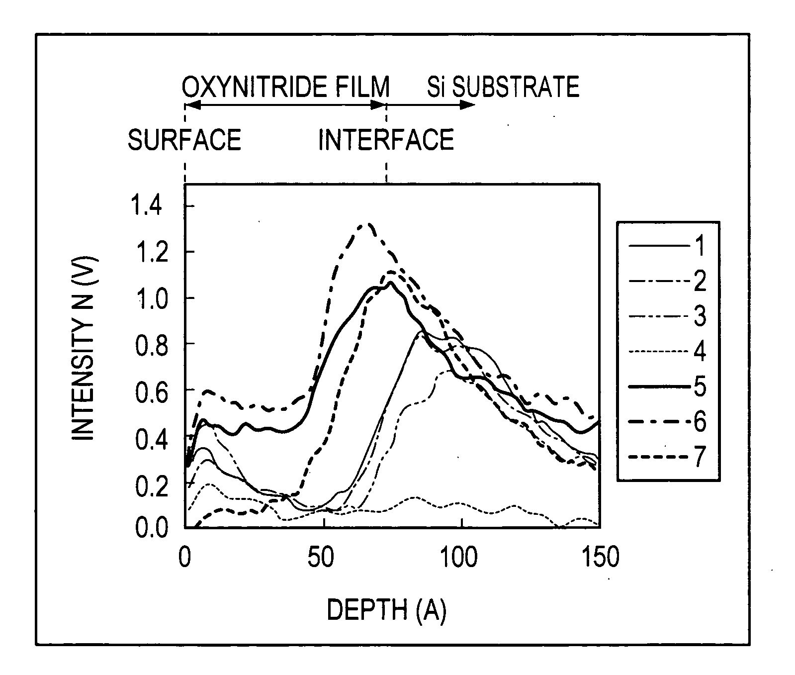
[0064]FIG. 7 shows distribution of the nitrogen in the direction of the thickness of the insulating film of thus-obtained semiconductor substrate according to the present invention. In FIG. 7, the horizontal axis denotes etching time. It is shown that it corresponds to the distance in the direction of the thickness of the insulating film, and more etching is applied as time passes to increase the distance and depth from the surface of the insulating film...


PUM

PropertyMeasurementUnit
Energyaaaaaaaaaa
Pressureaaaaaaaaaa
Pressureaaaaaaaaaa

Abstract

According to the present invention, plasma oxidation processing and plasma nitridation processing are applied at the same time to the surface of a semiconductor substrate by plasma using a microwave. After forming an insulating film by the plasma oxynitridation processing as described above, the plasma nitridation processing is further applied to the insulating film as necessary. Thereby, it is possible to form the insulating film with an excellent electrical characteristic.

Description

[0001] This is a continuation in part of PCT Application No. PCT / JP2004 / 001180, filed Feb. 5, 2004, which claims the benefit of a Japanese Patent Application No. 2003-029530, filed Feb. 6, 2003, all of which are incorporated herein by reference.BACKGROUND OF THE INVENTION [0002] 1. Field of the Invention [0003] The present invention relates to a plasma processing method forming an insulating film on the surface of a substrate by using plasma, a plasma processing apparatus for performing the plasma processing method, and a computer recording medium. [0004] 2. Description of the Related Art [0005] As an insulating film formed on a silicon substrate, a thermal oxide film formed by performing oxidation processing at high temperature of 1000° C. or higher has been often used conventionally. As microfabrication technology advances in recent years, it becomes necessary to reduce the thickness of this kind of oxide film (insulating film) in which reaction of Si and O progresses only by ther...

Claims


Application Information

Patent Timeline
IPC IPC(8): C23C8/02C23C8/28C23C8/34C23C8/36C30B33/00H01L21/314
CPCC23C8/02C23C8/28H01L21/3144C23C8/36C30B33/005C23C8/34A61P31/04H01L21/0214H01L21/02252H01L21/02249
Inventor KITAGAWA, JUNICHI
Owner TOKYO ELECTRON LTD
Why Eureka
Try Eureka