
Mold for nano imprinting

a mold and nanotechnology, applied in the field of nanoimprinting, can solve the problems of insufficient stability of the anti-adhesive layer according to jaszewski et al, damage to the replica, and residual polymer structure can contaminate the surface of the mold, so as to avoid any unwanted reactions and improve the density of the non-sticking functionality

Active Publication Date: 2005-12-29
OBDUCAT AB SE
View PDF13 Cites 1 Cited by
  • Summary
  • Abstract
  • Description
  • Claims
  • Application Information

AI Technical Summary

Benefits of technology

[0008] The term “nano-imprinting” should not be read as referring only to submicron structures, i.e. structures with a size in the range of 1-1000 nm. A mold often includes both submicron structures and structures with a size of up to 100 micron, and larger. The present invention is applicable for molds comprising submicron structures and / or micron structures. The best effect of the invention is observed with the submicron structures since these are relatively more sensitive to adhesion during mold release.
[0009] The present invention is based on the finding that a very firmly adhering monomolecular non-sticking layer can be obtained on the mold by subjecting the latter to a reaction with a fluoroalkyl compound having a mercapto group. This compound includes two principal groups, R and X. The first group, called R, has non-sticking properties. The second group, X, which is bound to the R-group, binds the compound, denoted RX, to the mold surface to form a monomolecular non-sticking layer.
[0010] According to one aspect of the invention, the mold is made of metal, such as nickel, chromium, etc and thus the non-sticking layer is formed by reaction with a fluoroalkyl compound having a mercapto group. The result of the reaction is a very strong layer comprising an organic sulfide of nickel in case of a nickel mold.
[0011] The R-group may include two subgroups; a first subgroup, called RA, that includes the non-sticking functionality, and a second subgroup, called RS, which serves as a “spacer”.
[0012] The first subgroup, RA, is a fluoroalkyl-containing group. The simplified representation of the RA-group is CnFmYp. C is carbon. The number of carbon atoms in RA is preferably n=1-20, more preferred n=1-10. F is fluorine. The number of fluorine atoms in RA is preferably m=1-30, more preferred m=3-20. Y may be hydrogen, oxygen, nitrogen, silicon or other atoms. In order to avoid any unwanted reactions with the surface of the mold Y is preferably hydrogen. The number of Y-atoms, p, is the number required to balance the RA-group with respect to its charge.
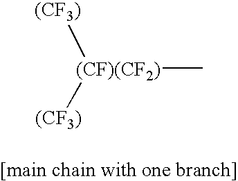
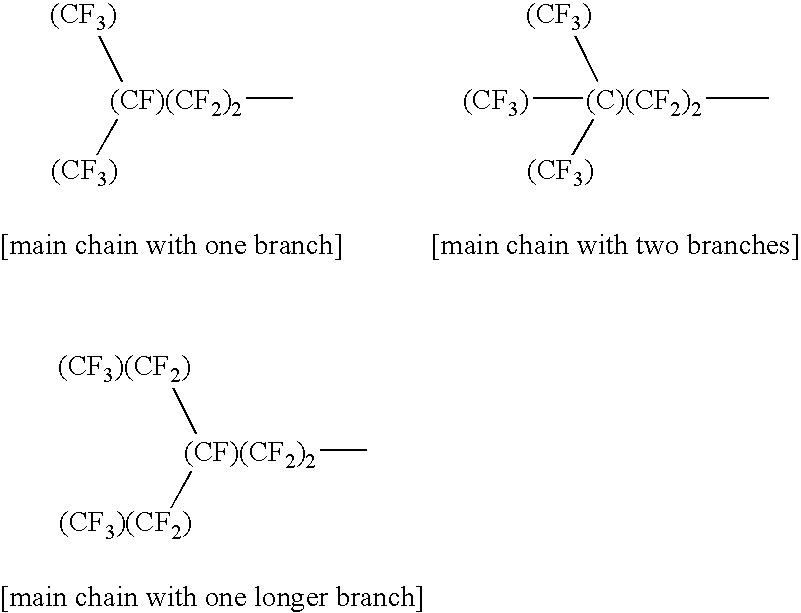
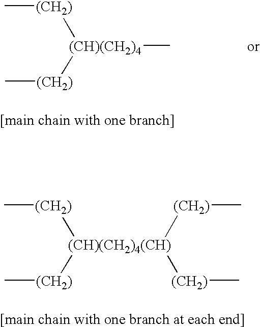
[0013] Each carbon atom in the RA-subgroup may be bound to 1-3 fluorine atoms. Preferably RA includes at least one perfluorinated carbon atom. Preferably the perfluorinated carbon atom is the terminal end carbon atom of the main chain of the RA-subgroup. RA may be linear or branched. For the non-sticking properties it is advantageous to have as many and as closely packed molecules of the RX-compound as possible bound to the surface of the mold. For reasons of close packing of the RX molecules the RA subgroup is preferably a linear chain, such as for example

Problems solved by technology

Adhesion during the mold release can cause damage to the replica.
Further, residual polymer structures can contaminate the surface of the mold.
Thus, it seems that the anti-adhesive layer according to Jaszewski et al is not sufficiently stable.

Method used


Image

  • Mold for nano imprinting
  • Mold for nano imprinting
  • Mold for nano imprinting

Examples


example 1

[0032] A silicon mold was etched to define a certain nano structure. The surface of the mold was then coated with a thin layer of nickel. The mold was cleaned in heptane.

[0033] A fluoroalkyl compound having a mercapto group, which compound was 1H, 1H, 2H, 2H-perfluorooctanethiol and had the structure:

CF3 (CF2)5 (CH2)2SH

was dissolved in heptane to obtain a 2% solution. The temperature of the solution was about 20° C. The cleaned metal mold was put into an agitated beaker containing the solution. The mold was now provided with a monomolecular non-sticking layer with the structure:

CF3 (CF2)5(CH2)2S—Ni

The mold was taken up from the beaker and was cleaned by dipping it in each of three consecutive beakers each containing heptane. The mold was then heated to 70° C. whereby the heptane was evaporated. The mold was tested in a nano-imprint lithography process and it was found that the mold withstood more than 50 imprint sequences without any detectable degradation.

[0034] The example...

example 2

[0035] The same RX-compound as described in example 1 was applied to a mold similar to that used in example 1. The mold was cleaned in heptane and then put into an oven that had a temperature of 110° C., a nitrogen atmosphere and a pressure of 75 mbar. Pure RX-compound was injected into the oven. The mold, now provided with a monomolecular non-sticking layer with a structure similar to that described in example 1, was taken out of the oven and was cleaned by dipping it in each of three consecutive beakers each containing heptane. Finally, the mold was dried by heating it to 70° C. Similar results as in example 1 were obtained upon testing.


PUM

PropertyMeasurementUnit
Thicknessaaaaaaaaaa
Thicknessaaaaaaaaaa
Covalent bondaaaaaaaaaa

Abstract

A metal mold for use in a nano-imprinting process comprises a firmly adhering monomolecular non-sticking layer. The later was obtained by subjecting the mold to a reaction with a fluoroalkyl compound having a mercapto group. As a result of said reaction, the layer comprises an organic sulfide of said metal.

Description

TECHNICAL FIELD OF THE INVENTION [0001] The present invention relates to nano-imprinting in general and especially to a mold for nano-imprinting. BACKGROUND ART [0002] In the replication of nanostructures by hot embossing it is necessary to provide a non-sticking interface between the nanostructured master and the thermoplastic to be embossed. This allows demolding without degrading the replication fidelity. Adhesion during the mold release can cause damage to the replica. Further, residual polymer structures can contaminate the surface of the mold. A prerequisite for a successful imprint process is that the mold used should be chemically and mechanically stable and also adhere poorly with polymers to avoid sticking thereof to the mold. [0003] R. W. Jaszewski, et al disclose in Microelectronic Engineering 35 (1997) 381-384 covering the surface of the mold with an ultra-thin anti-adhesive layer comprising a polytetrafluorethylene (PTFE) film. The film is deposited according to two ki...

Claims


Application Information

Patent Timeline
IPC IPC(8): B29C33/42B29C33/56B41MB41M1/06B81C1/00G03F7/00G11B5/855G11B7/24047H01L21/31H01L21/469
CPCB29C33/424B29C33/56B82Y10/00G11B5/855G03F7/0002G03F7/0017B82Y40/00
Inventor LING, TORBJORNMONTELIUS, LARSKEIL, MATTHIASBECK, MARC
Owner OBDUCAT AB SE
Learn More