Thick film capacitors, embedding thick-film capacitors inside printed circuit boards, and methods of forming such capacitors and printed circuit boards

a thick film capacitor and printed circuit board technology, applied in the direction of variable capacitors, stacked capacitors, printed circuit non-printed electric components association, etc., can solve the problems of many capacitors being shorted after etching, capacitor dielectric glass and dopants being attacked and dissolved, capacitor dielectrics may be shorted, etc., to reduce the resultant dielectric constant, reduce the risk of shortening, and improve the reliability and performance of capacitors

Active Publication Date: 2006-01-05
CHEMTRON RES
View PDF10 Cites 49 Cited by
  • Summary
  • Abstract
  • Description
  • Claims
  • Application Information

AI Technical Summary

Benefits of technology

[0013] According to the above embodiments, a protective coating protects all or a part of a dielectric of a capacitor from etching solutions used during fabrication. The etching solutions would otherwise attack and dissolve the dielectric glasses and dopants present in the dielectri

Problems solved by technology

However, etching solutions common in the printed circuit board industry, such as ferric chloride in hot 2.4 normal hydrochloric acid, may attack and dissolve the capacitor dielectric glass and dopants.
Etching solutions damage capacitor dielectrics such that many capacitors may be shorted after etching.
Even when shorting has not occurred, the damage to the dielectric may compromise the long term reliability of the capacitor, especially if all of the etching solution has not been thoroughly removed from the capacitor.
Other solutions commonly used in the printed c

Method used


Image

  • Thick film capacitors, embedding thick-film capacitors inside printed circuit boards, and methods of forming such capacitors and printed circuit boards
  • Thick film capacitors, embedding thick-film capacitors inside printed circuit boards, and methods of forming such capacitors and printed circuit boards
  • Thick film capacitors, embedding thick-film capacitors inside printed circuit boards, and methods of forming such capacitors and printed circuit boards

Examples


Embodiment Construction

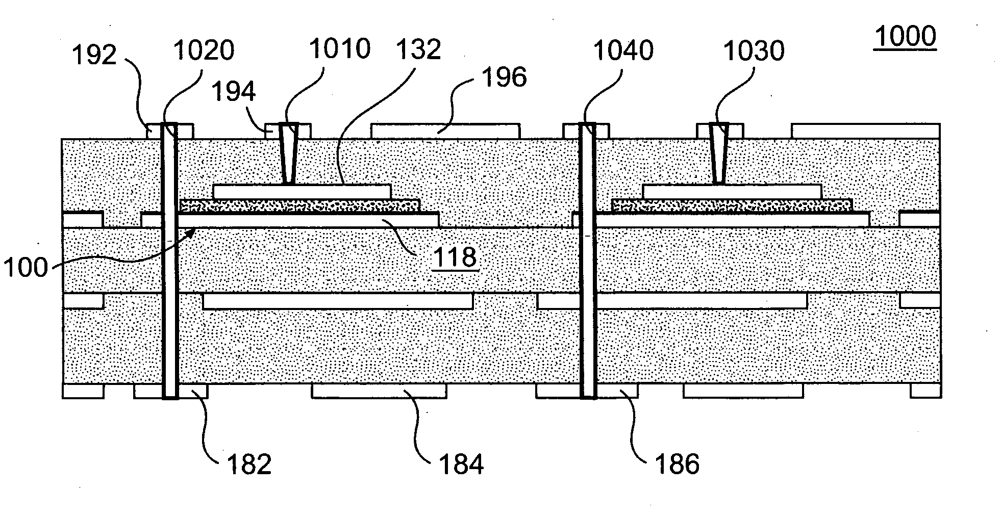
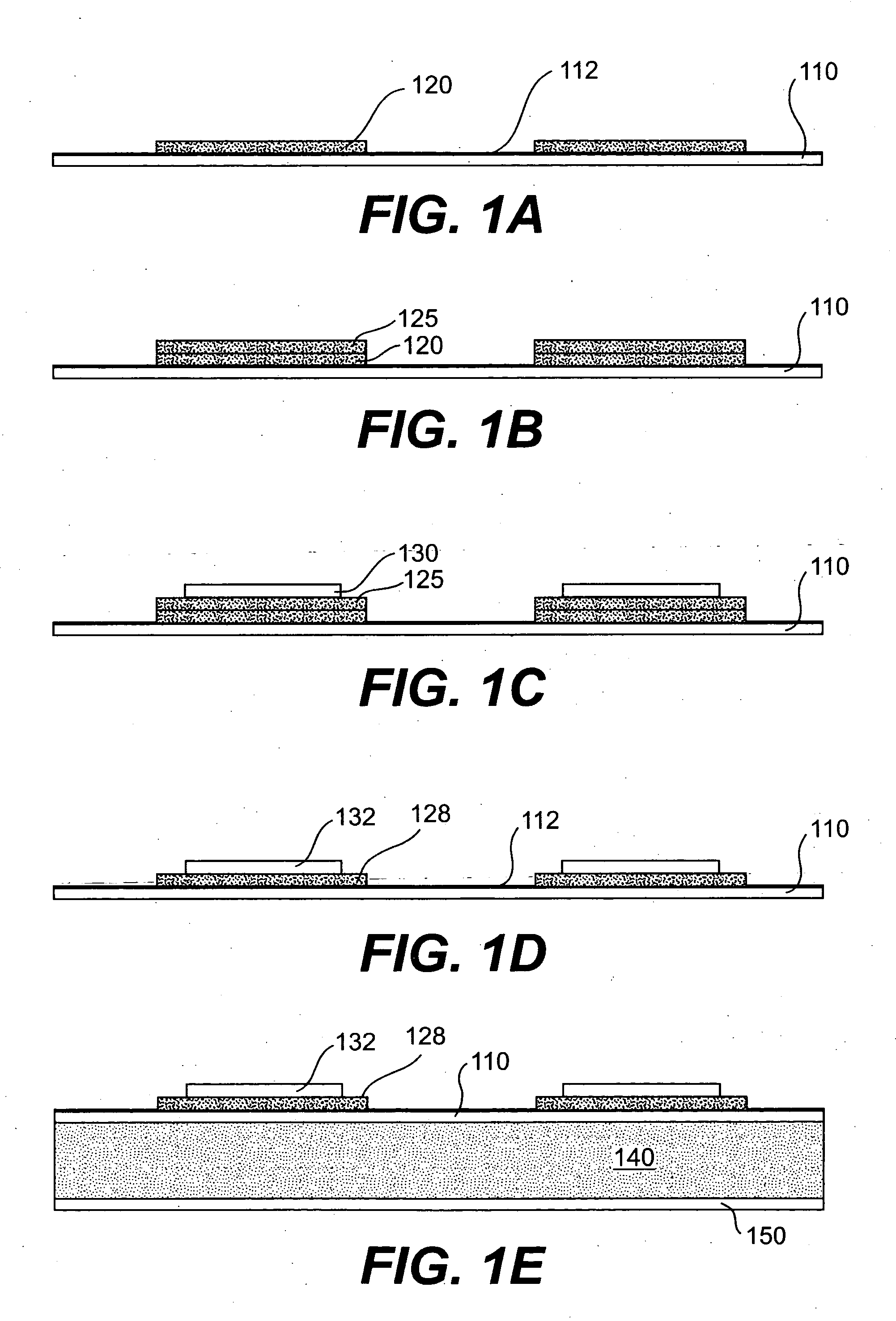
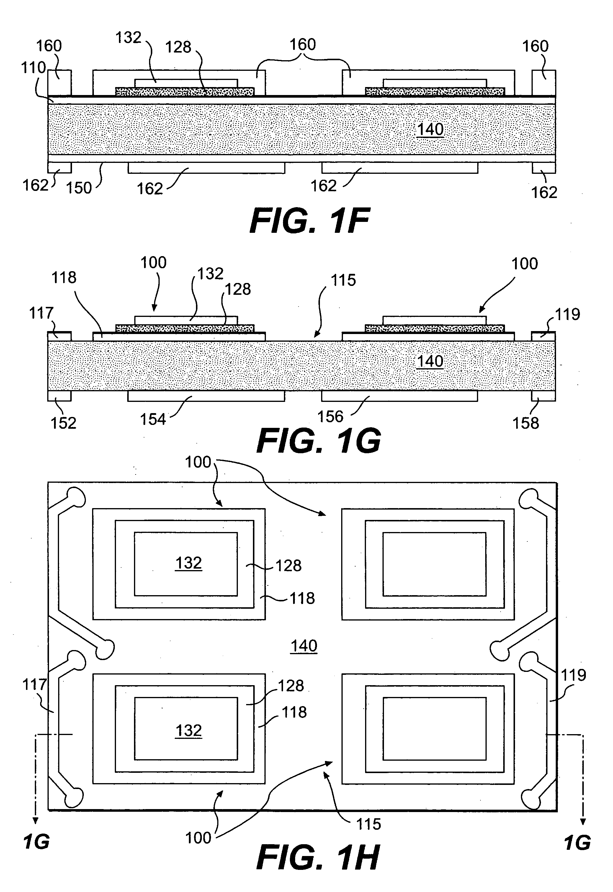
[0020]FIGS. 1A-1J illustrate a first method of manufacturing a multilayer printed circuit board (PCB) 1000 (FIG. 1J) with embedded capacitors having a single-layer capacitor on metallic foil design. For illustrative purposes, four embedded capacitors are illustrated as formed in FIGS. 1A-1J (only two capacitors are visible in the sectional views FIGS. 1A-1G and 1I-1J). However, one, two, three, or more capacitors can be formed on a foil by the methods described in this specification. The following written description is addressed to the formation of only one of the illustrated capacitors for the sake of simplicity. FIGS. 1A-1G and 1I-1J are sectional views in front elevation. FIG. 1G is a cross section taken on line 1G-1G in FIG. 1H. FIG. 1H is a top plan view showing four embedded capacitors 100.

[0021] In FIG. 1A, a metallic foil 110 is provided. The metallic foil 110 may be of a type generally available in the industry. For example, the metallic foil 110 may be copper, copper-inv...


PUM

PropertyMeasurementUnit
Dielectric polarization enthalpyaaaaaaaaaa
Metallic bondaaaaaaaaaa

Abstract

A method of embedding thick-film capacitors includes covering capacitor layers with a protective coating prior to etching to prevent etching solutions from coming in contact with and damaging the capacitor layers.

Description

BACKGROUND [0001] 1. Technical Field [0002] The technical field is thick film capacitors, in general. More particularly, embedded capacitors in printed circuit boards. Still more particularly, the technical field includes embedded capacitors in printed circuit boards made from thick film dielectrics. [0003] 2. Related Art [0004] The practice of embedding capacitors in printed circuit boards (PCB) allows for reduced circuit size and improved circuit performance. Capacitors are typically embedded in panels that are stacked and connected by interconnection circuitry, the stack of panels forming a printed circuit board. The stacked panels can be generally referred to as “innerlayer panels.”[0005] Passive circuit components embedded in printed circuit boards formed by fired-on-foil technology are known. “Separately fired-on-foil” capacitors are formed by depositing a thick-film capacitor material layer onto a metallic foil substrate, followed by depositing a top electrode material over t...

Claims


Application Information

Patent Timeline
IPC IPC(8): H05K1/18H01G7/00H01G4/33H01L21/02H01L27/00
CPCH05K1/162H05K3/061H05K3/429H05K2201/0355H05K2201/09509Y10T29/49155Y10T29/417Y10T29/49165Y10T29/49117Y10T29/4913Y10T29/43H05K2201/09763H05K1/16
Inventor BORLAND, WILLIAM J.FERGUSON, SAULPYADA, HENA
Owner CHEMTRON RES
Why Eureka
Try Eureka