Ultrathin module for semiconductor device and method of fabricating the same

a technology of ultrathin modules and semiconductor devices, applied in microstructural devices, microstructured devices, printing, etc., can solve the problems of less power consumption and less cost of cmos image sensors, and achieve the effect of easy mass production

Inactive Publication Date: 2006-01-12
SAMSUNG ELECTRONICS CO LTD
View PDF4 Cites 58 Cited by
  • Summary
  • Abstract
  • Description
  • Claims
  • Application Information

AI Technical Summary

Benefits of technology

[0012] Another object of the present invention is to provide an ultrathi

Problems solved by technology

While the CCD is relatively superior in terms of image quality and nois

Method used


Image

  • Ultrathin module for semiconductor device and method of fabricating the same
  • Ultrathin module for semiconductor device and method of fabricating the same
  • Ultrathin module for semiconductor device and method of fabricating the same

Examples


Embodiment Construction

[0031] The present invention will now be described more fully hereinafter with reference to the accompanying drawings. In this disclosure, well-known structures and processes are not described or illustrated in detail for the sake of clarity. Furthermore, the drawings are not to scale. Rather, the relative dimensions of some of the elements may be exaggerated for simplicity and clarity of illustration. Still further, like reference numerals are used to designate like and corresponding parts throughout the drawings.

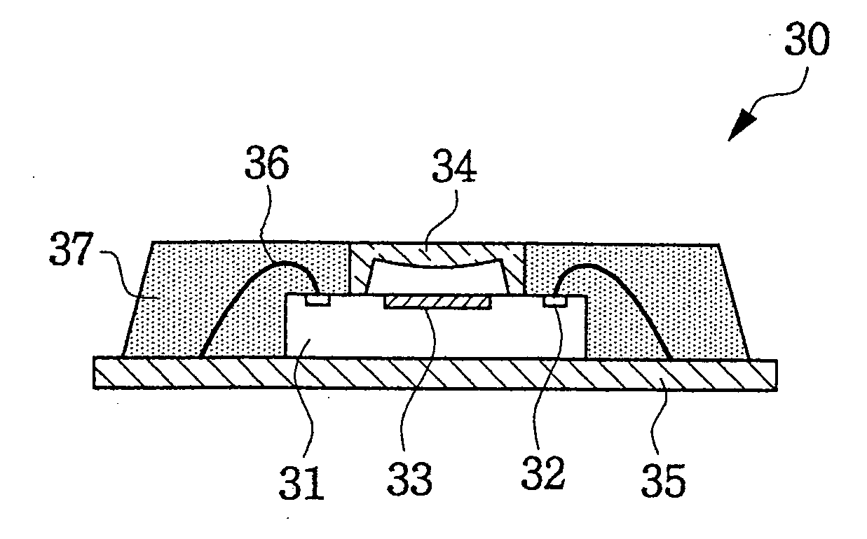
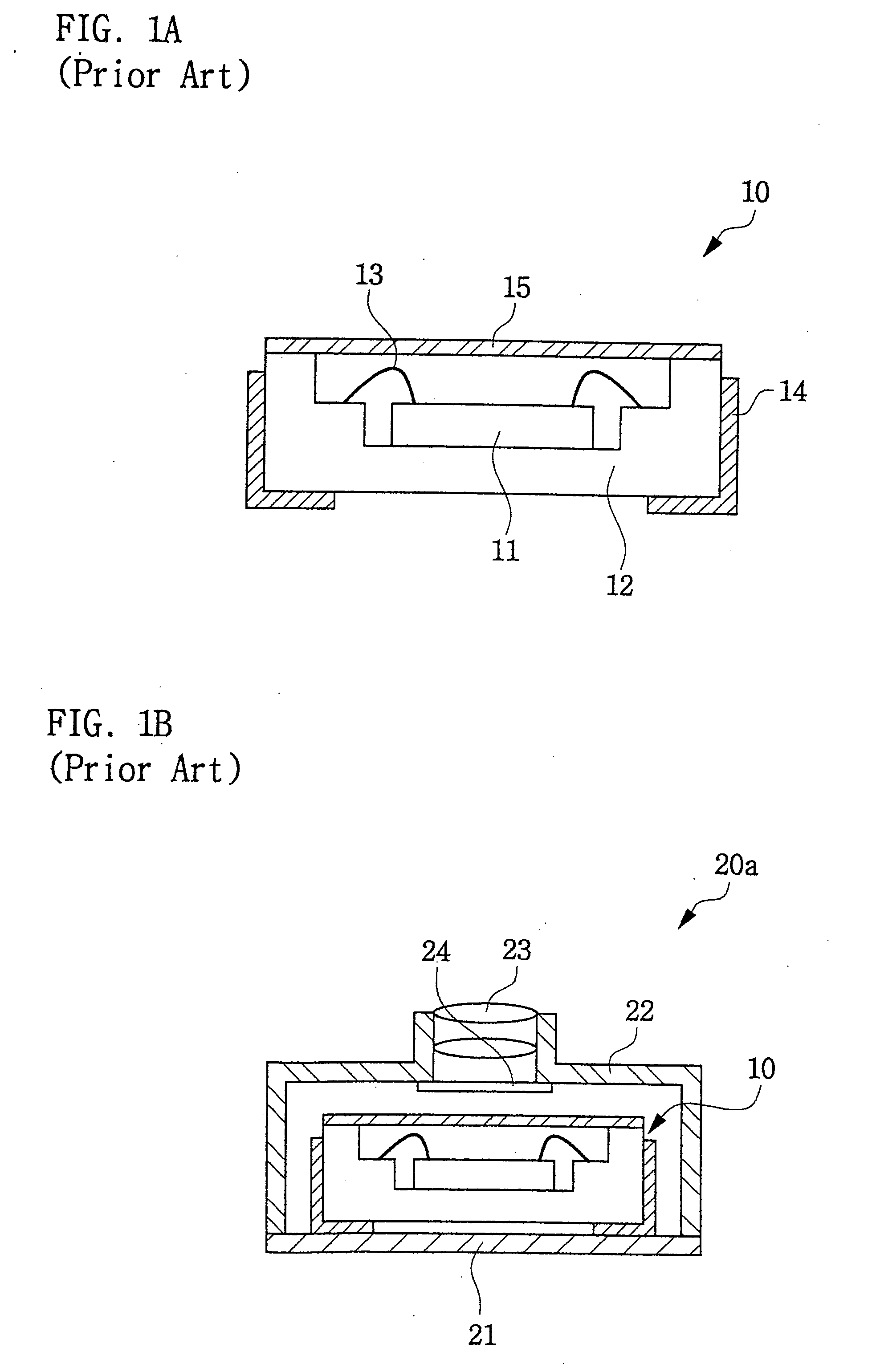
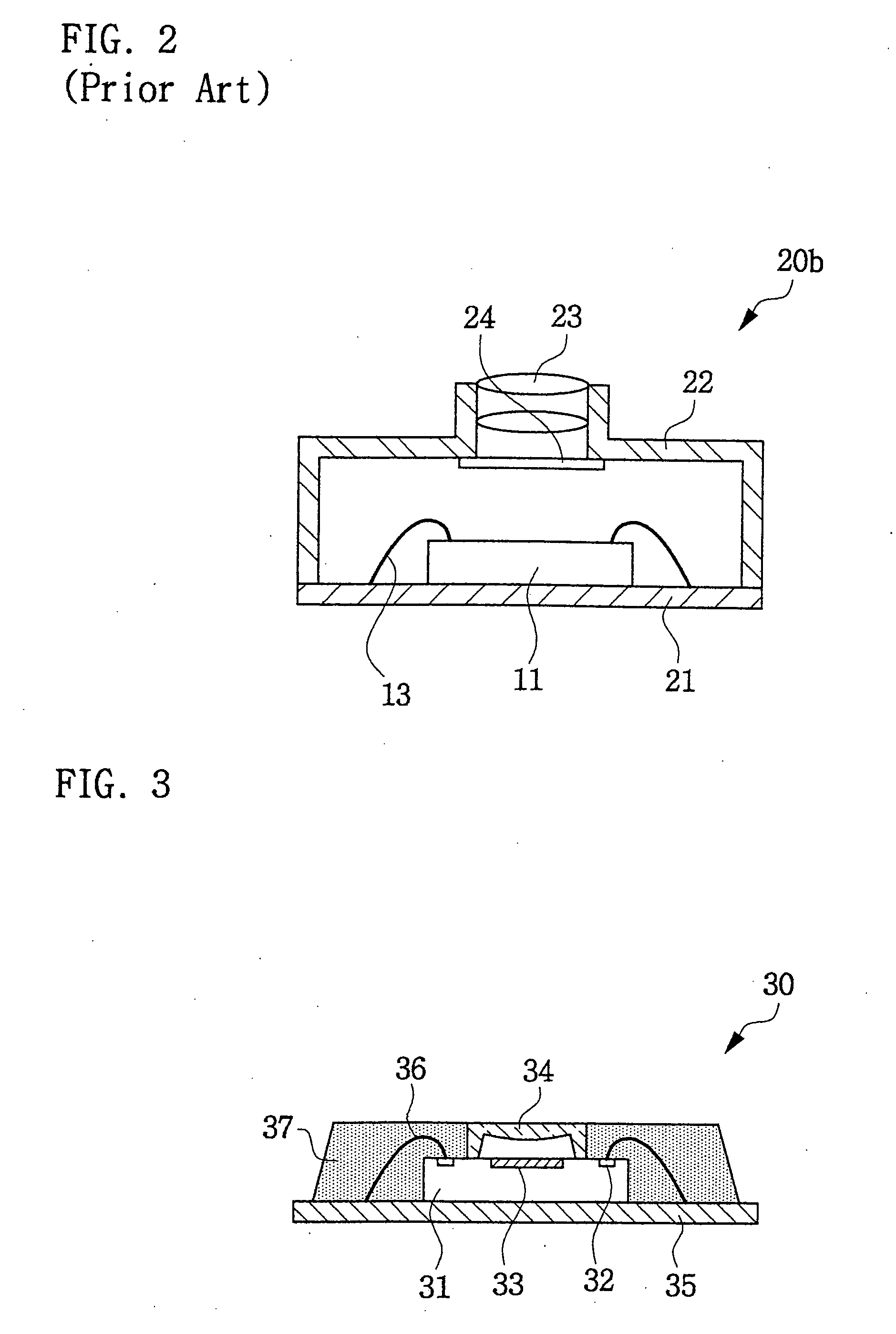
[0032] Referring now to FIGS. 3 to 5, each ultrathin module 30, 40 and 50 includes a semiconductor chip 31 that is directly attached to a top surface of a module substrate 35 or 45. The semiconductor chip 31 has a number of input / output (I / O) pads 32 disposed along the periphery of on an active surface thereof. Furthermore, the semiconductor chip 31 has a specific region 33 at the center of the active surface that needs protection. Although not shown in drawings, another ...


PUM

PropertyMeasurementUnit
Areaaaaaaaaaaa
Translucencyaaaaaaaaaa
Transparencyaaaaaaaaaa

Abstract

An ultrathin module is provided for special types of semiconductor devices such as image sensor devices and micro-electro-mechanical system (MEMS) devices. In the module, a chip cover is directly attached to a semiconductor chip so as to protect a light-sensing area or mechanical elements of the chip. The chip cover may also be used as a lens assembly and an infrared light filter. In a fabrication method, the chips are provided on a wafer, and the chip covers are attached to the chips, respectively, before the wafer is sliced to separate the chips from one another.

Description

BACKGROUND OF THE INVENTION [0001] 1. Field of the Invention [0002] The present invention relates generally to electronic packaging technology. More particularly, the present invention relates to special types of semiconductor devices, such as image sensor devices and micro-electro-mechanical system (MEMS) devices, and to an ultrathin module comprising such devices. [0003] 2. Description of the Related Art [0004] Recently, enhanced imaging technology has produced superior image quality not only for high-resolution camera phones, but also for current and emerging industrial applications that require cost-effective image-capturing solutions. This enhanced imaging technology often resides in an image sensor module. The image sensor module contains an image sensor capable of converting optical images into electric signals. [0005] More specifically, the image sensor comprises an array of pixels, and acquires an image when light is incident on the array of pixels. The pixels change the ph...

Claims


Application Information

Patent Timeline
IPC IPC(8): H01L23/02H01L21/44B81B7/02B81C3/00H01L27/14H04N5/335
CPCB81B7/0067H01L23/315H01L2924/1461H01L2924/10253H01L2924/1815H01L2224/48091H01L24/48H01L27/14618H01L27/14625H01L27/14636H01L31/0203H01L31/0232H01L2224/48227H01L2224/48247H01L2924/16235H01L2924/3025H01L2924/00014H01L2924/00H01L24/45H01L31/02325H01L2224/451H01L2924/14H01L2924/16151H01L2924/16195H01L2924/181H01L2924/00015H01L2224/05599H01L2924/00012H01L23/00H01L27/14
Inventor ROH, KWON-YOUNGMOK, SEUNG-KON
Owner SAMSUNG ELECTRONICS CO LTD
Why Eureka
Try Eureka