Light emitting diode structure and method for fabricating the same

a technology of light-emitting diodes and diodes, which is applied in the direction of discharge tubes/lamp details, discharge tubes luminescnet screens, electric discharge lamps, etc., can solve the problems of insufficient light efficiency, complicated process, and inability to manufacture led, so as to reduce total reflection, reduce horizontal light propagation between substrate and semiconductor layer, and increase the light extraction efficiency of led elements

Inactive Publication Date: 2009-06-25
TEKCORE CO LTD
View PDF7 Cites 50 Cited by
  • Summary
  • Abstract
  • Description
  • Claims
  • Application Information

AI Technical Summary

Benefits of technology

[0012]The advantage of the present invention is to use a novel process to form a chemical reaction layer on the carved regions, and use the chemical reaction layer as a natural etching mask to form an irregular geometry of serrations on the carved regions via a dry- or wet-etching method. Then, a semiconductor light emitting element is epitaxially grown with irregular serrations naturally formed on the border of the semiconductor light emitting element. The light generated by the LED element will be scattered or diffracted by the irregular serrations. Thus, the horizontal light propagation between the substrate and the semiconductor layers is decreased, and the total reflection is reduced, and the light extraction efficiency of the LED element is increased. Further, the present invention has a simple process and thus can reduce fabrication cost and benefit mass-production.

Problems solved by technology

Thus, LED has an insufficient light efficiency.
However, such a process is more complicated and cost-inefficient, which will impair the commercialization of LED.

Method used


Image

  • Light emitting diode structure and method for fabricating the same
  • Light emitting diode structure and method for fabricating the same
  • Light emitting diode structure and method for fabricating the same

Examples


Embodiment Construction

[0018]The technical contents of the present invention will be described with the embodiments. However, it should be noted that the embodiments are only to exemplify the present invention but not to limit the scope of the present invention.

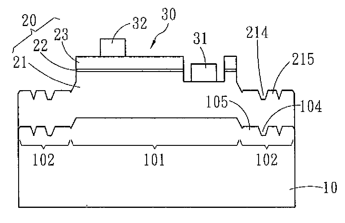
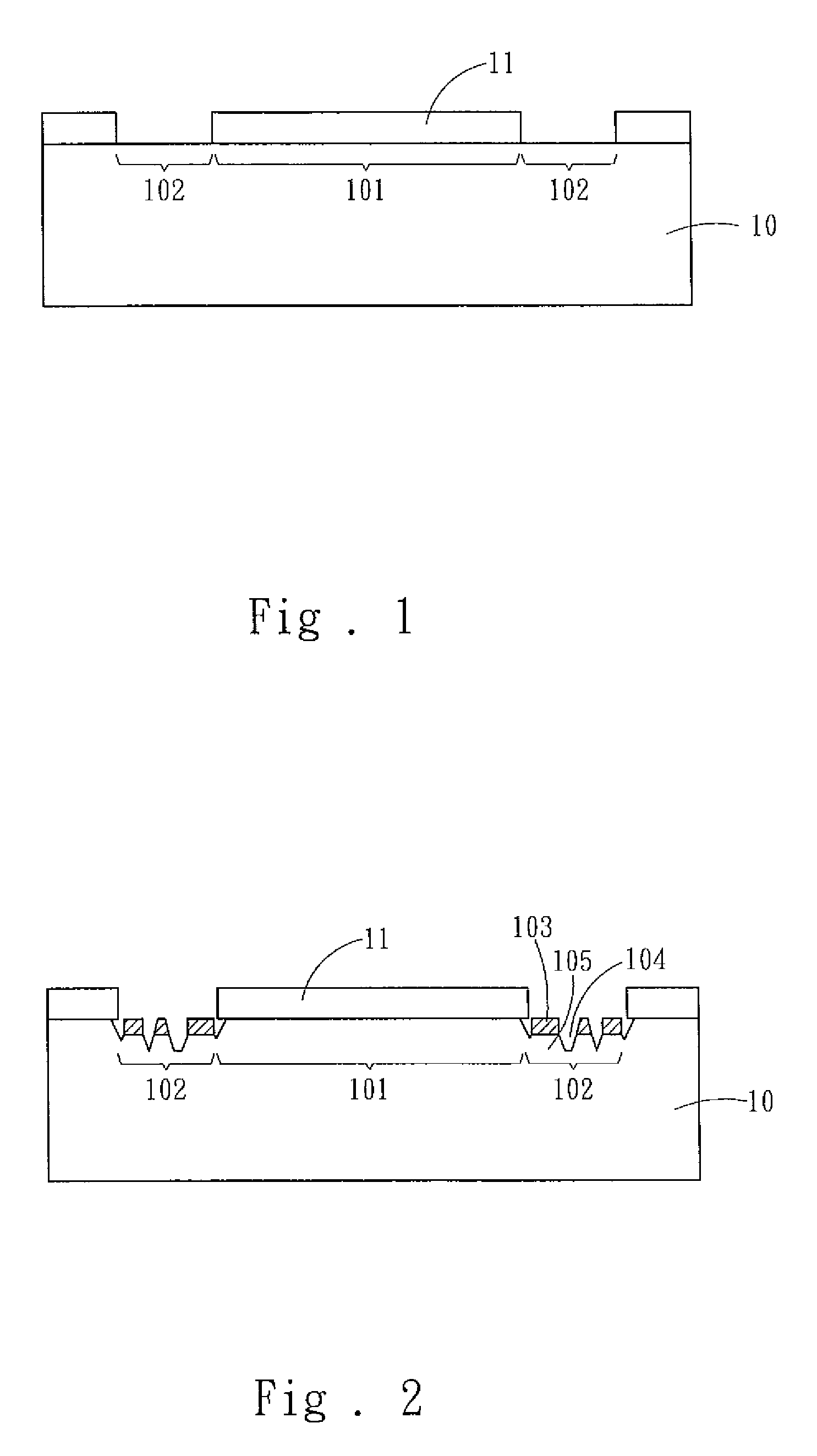
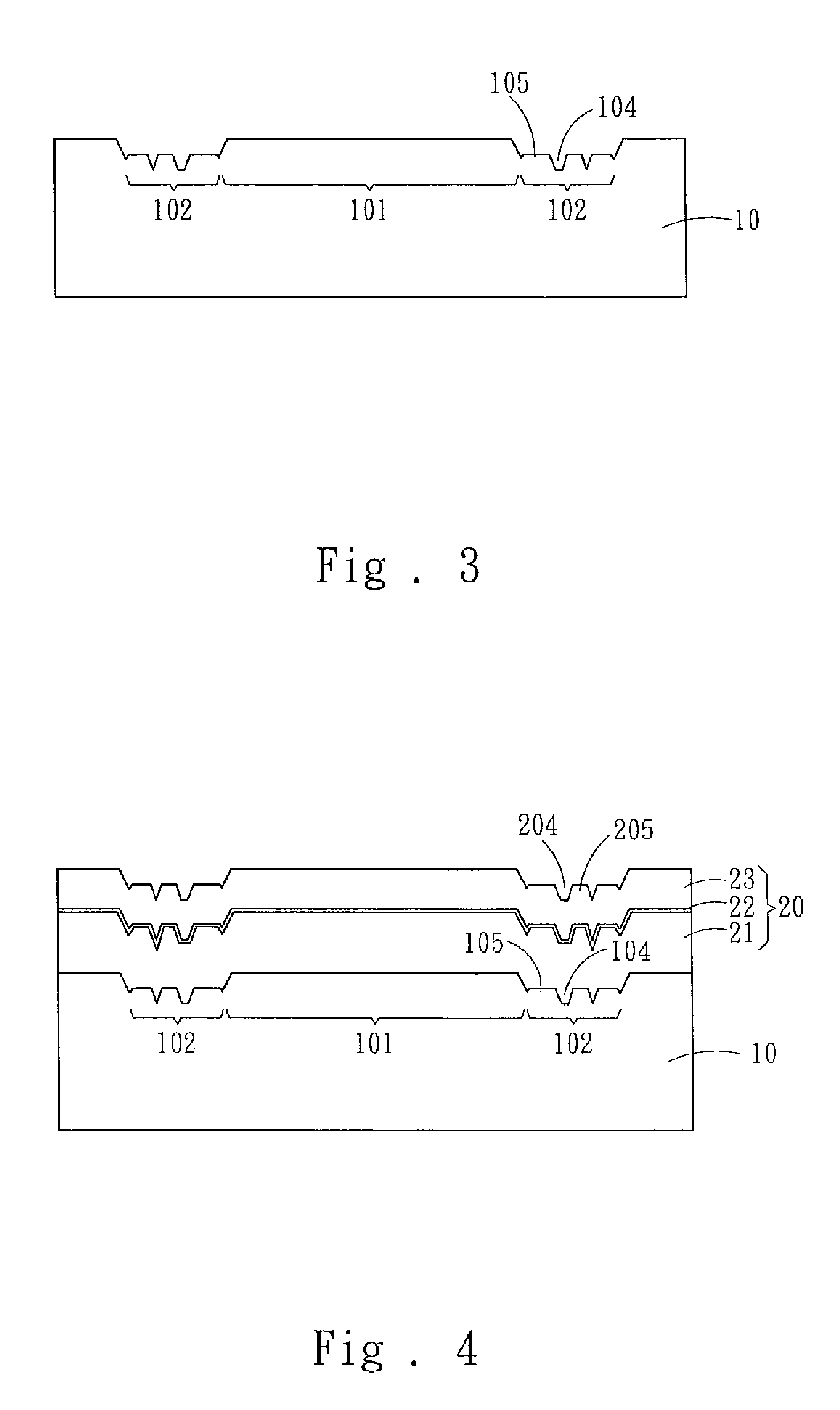
[0019]Refer to from FIG. 1 to FIG. 5. In the method for fabricating a light emitting diode structure of the present invention, a substrate 10 is provided firstly. The substrate 10 may be made of sapphire (Al2O3), silicon carbide (SiC), silicon (Si), gallium arsenide (GaAs), aluminum nitride (AlN), or gallium nitride (GaN). A passivation layer 11 is grown on the surface of the substrate 10. The passivation layer 11 is patterned to define element regions 101 covered by the passivation layer 11, and carved regions 102 where the surface of the substrate 10 is exposed, as shown in FIG. 1.

[0020]Next, the substrate 10 is placed in a first solution for chemical reaction, and a high-density chemical reaction layer 103 naturally forms on the surface of the s...


PUM


Abstract

The present invention discloses a light emitting diode structure and a method for fabricating the same. In the present invention, a substrate is placed in a solution to form a chemical reaction layer on carved regions; the carved region is selectively etched to form a plurality of concave zones and form a plurality of convex zones; a semiconductor layer structure is epitaxially grown on the element regions and carved regions of the substrate; the semiconductor layer structure on the element regions is fabricated into a LED element with a photolithographic process.

Description

FIELD OF THE INVENTION[0001]The present invention related to a light emitting diode structure and a method for fabricating the same, particularly to a light emitting diode structure and a method for fabricating the same, wherein concave zones and convex zones are formed on the surface of each carved region.BACKGROUND OF THE INVENTION[0002]Improving LED (Light Emitting Diode) light efficiency is a top priority for realizing a solid-state illuminator. There are two approaches to improve LED light efficiency: one is to increase LED internal quantum efficiency, and the other is to increase LED external quantum efficiency (LED light extraction efficiency).[0003]There is a great difference between the refractive indexes of a semiconductor and a packaging material; therefore, a LED usually has a small total reflection critical angle. The light generated by LED reaching an interface by an angle greater than the total reflection critical angle will be totally reflected back to the interior o...

Claims


Application Information

Patent Timeline
Patent Type & Authority Applications(United States)
IPC IPC(8): H01L21/306H01L33/00H01L33/22
CPCH01L33/22
Inventor LIN, HUNG-CHENGLEE, CHIA-MINGCHYI, JEN-INN
Owner TEKCORE CO LTD
Why Eureka
Try Eureka