System and method for searching for patterns of semiconductor wafer features in semiconductor wafer data

Inactive Publication Date: 2006-01-12
ADE CORPORATION
View PDF3 Cites 47 Cited by
  • Summary
  • Abstract
  • Description
  • Claims
  • Application Information

AI Technical Summary

Benefits of technology

[0013] The integration of wafer data management, process monitoring, data analysis, and data automation into one system allows improved metrology and inspection tool use, allowing for surface inspection and characterization of both thin film devices and bare wafers with the same system.

Problems solved by technology

However, with the wide variety of and large amounts of data from the numerous tools used in the manufacturing of semiconductor wafer and integrated circuits, managing, analyzing and automating wafer data has become extremely complicated.
In the past, wafer data management and analysis systems have been developed for dimensional systems, but they have not included data from surface inspection systems such as defect evaluation systems.
Defect evaluation systems were developed, but they did not support wafer characterization tools or automation features.
Because the disparities between the data from the numerous systems, the ability of engineering

Method used


Image

  • System and method for searching for patterns of semiconductor wafer features in semiconductor wafer data
  • System and method for searching for patterns of semiconductor wafer features in semiconductor wafer data
  • System and method for searching for patterns of semiconductor wafer features in semiconductor wafer data

Examples


Embodiment Construction

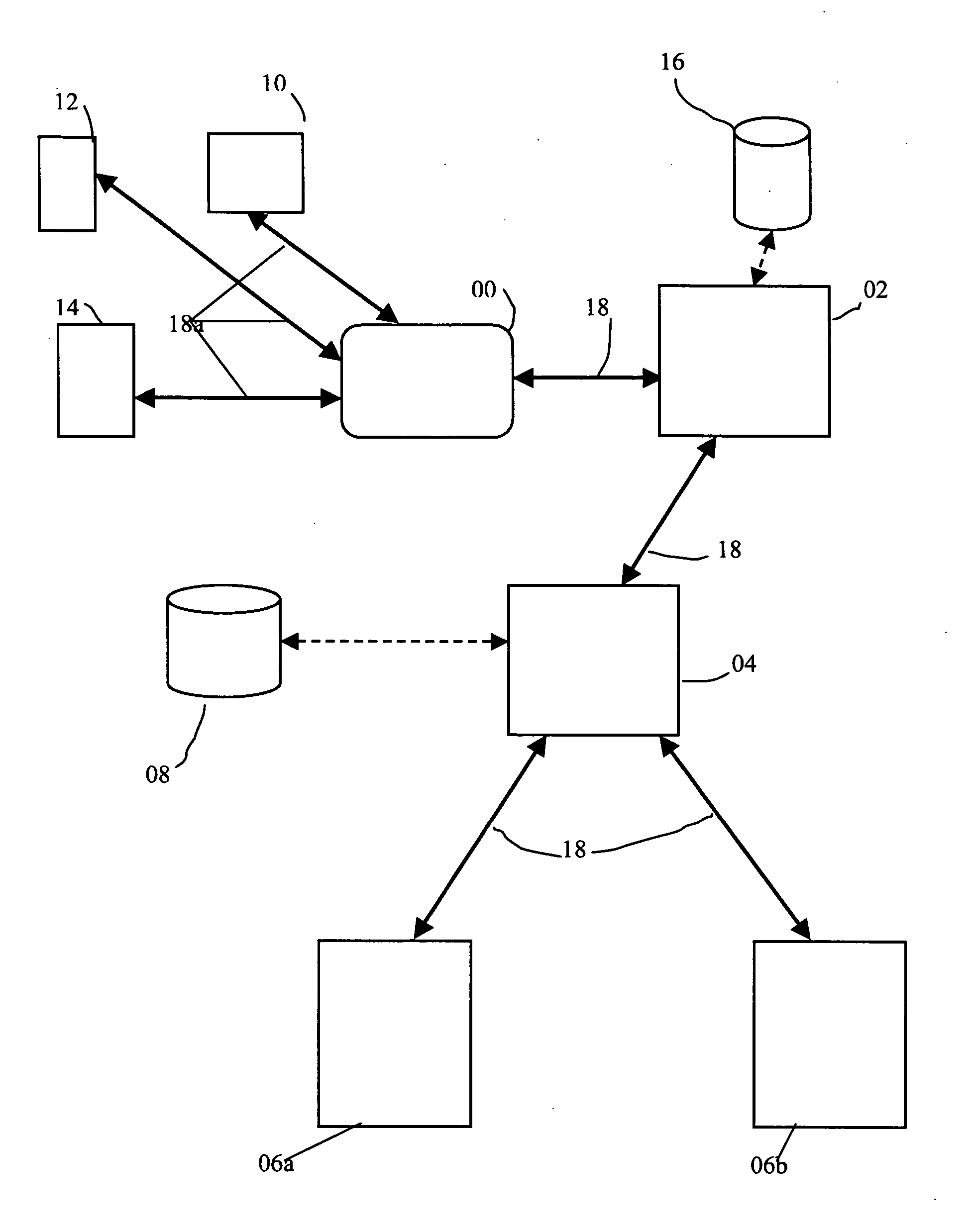
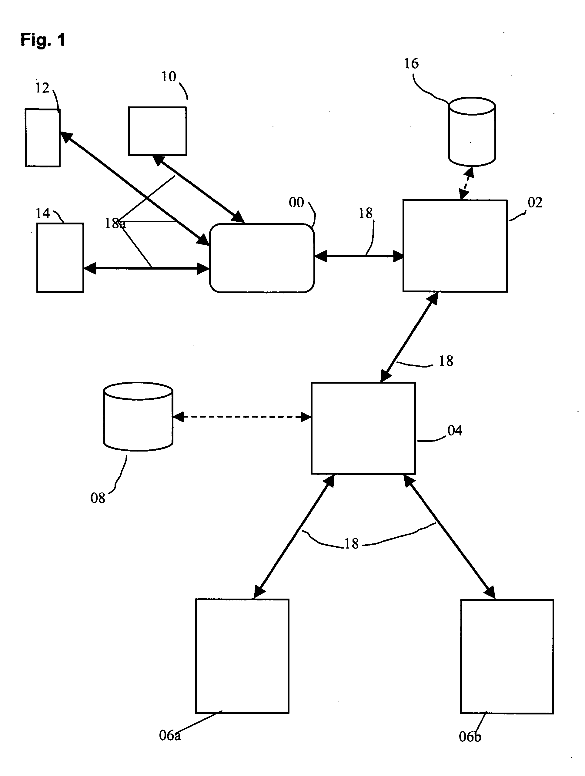
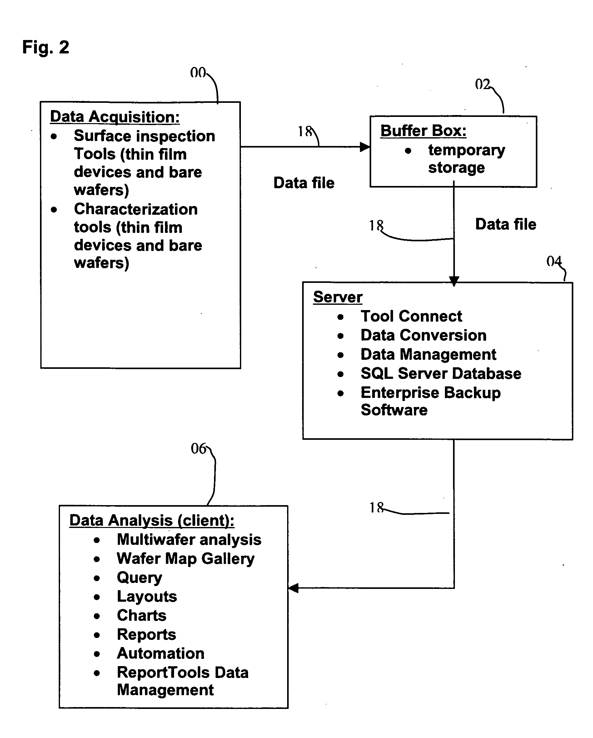
[0074] As seen in FIG. 1, the present invention comprises a data acquisition system 00 for acquiring semiconductor wafer scan data from metrology and inspection tools such as wafer dimensional scanning tool 10, device inspection tool 12 and nanotopography tool 14. Each tool communicates with data acquisition system 00 using its own communications or interface protocol, over a communications path 18a. Data acquisition system 00, in turn, communicates over a communications path 18 with buffer system 02. Buffer system 02 provides temporary storage 16 for scan data transmitted from the wafer scanning tools and also provides fault tolerance features. Still in FIG. 1, buffer system 02 transmits data to server system 04 over communications path 18. Server system 04 provides storage for scan data transmitted by buffer system 02 in a database management system 08. Server system 04 converts the scan data into a format used by data management system 08.

[0075] Still in FIG. 1, server system 04...


PUM


Abstract

A system for searching for patterns of semiconductor wafer features for use in silicon manufacturing and device fabrication processes, the system including: a data acquisition system 00 for acquiring scan data from differing types of semiconductor wafer scanning tools such as wafer dimensional tools 10, wafer inspection tools 12, and wafer nanotopography tools 14; a buffer system 02 for providing temporary storage for scan data transmitted and for providing fault tolerance; a server system 04 for providing storage for the scan data transmitted from the buffer system 02 and converting the scan data into a format used by and stored in a database 08 management system; an analysis system 06 client station including a display and communicating with the server system 04, the analysis system 06 and the server system 04 providing scan data structuring and query operations and data transfer operations.

Description

TECHNICAL FIELD [0001] The present invention is directed to the field of materials processing, and more particularly to a system and method for searching for patterns of semiconductor wafer features in semiconductor wafer data. BACKGROUND [0002] The manufacturing of semiconductor wafer and integrated circuits has traditionally employed several types of systems and tools to provide quality control and process monitoring. [0003] For example, wafer geometry systems, ranging from the tabletop gauges to high volume multi-functional sorting systems on state of the art robotic transfer platforms, are used to obtain wafer characterization data to provide an accurate knowledge of wafer dimensional characteristics such as flatness, diameter, thickness, bow, warp, shape, nanotopography, resistivity, backgrind characteristics, thermal shape change, among others. In addition, surface inspection systems are used to identify defects occurring on a surface of a semiconductor wafer, such as particle...

Claims


Application Information

Patent Timeline
IPC IPC(8): G06F17/50G06F19/00G01M99/00
CPCG01N21/9501G06F17/30554G06Q10/06G05B19/41875H01L21/67005H01L21/67253G05B2219/2602G06Q50/04Y02P90/30G06F16/248Y02P90/02
Inventor KECK, JAYKALLUS, DAVID M.SMITH, BRYAN W.VERGOW, ZACHARY J.
Owner ADE CORPORATION
Why Eureka
Try Eureka