

High energy, real time capable, direct radiation conversion X-ray imaging system for Cd-Te and Cd-Zn-Te based cameras
a technology of cd-te and cd-zn-te, which is applied in the field of high energy charge integration imaging devices, can solve the problems of preventing any increase in accuracy, increasing the time of pixel charge integration, and reducing the image frame acquisition rate, so as to achieve high energy and high image frame acquisition rate. , the effect of high energy
- Summary
- Abstract
- Description
- Claims
- Application Information
AI Technical Summary
Benefits of technology
Problems solved by technology
Method used
Image

Examples
Embodiment Construction
[0031] Referring now to the drawings, the details of preferred embodiments of the present invention are graphically and schematically illustrated. Like elements in the drawings are represented by like numbers, and any similar elements are represented by like numbers with a different lower case letter suffix.
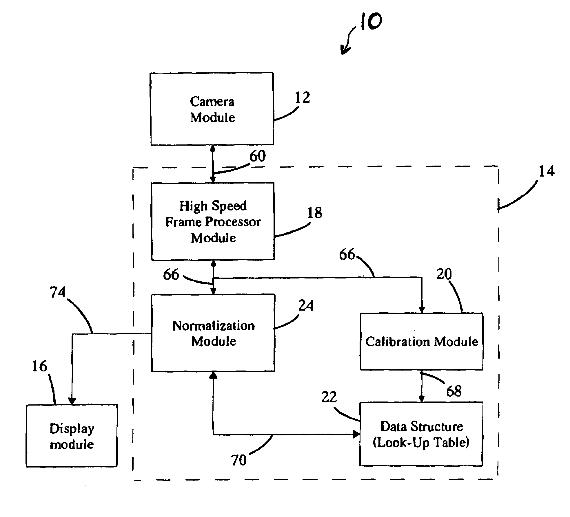
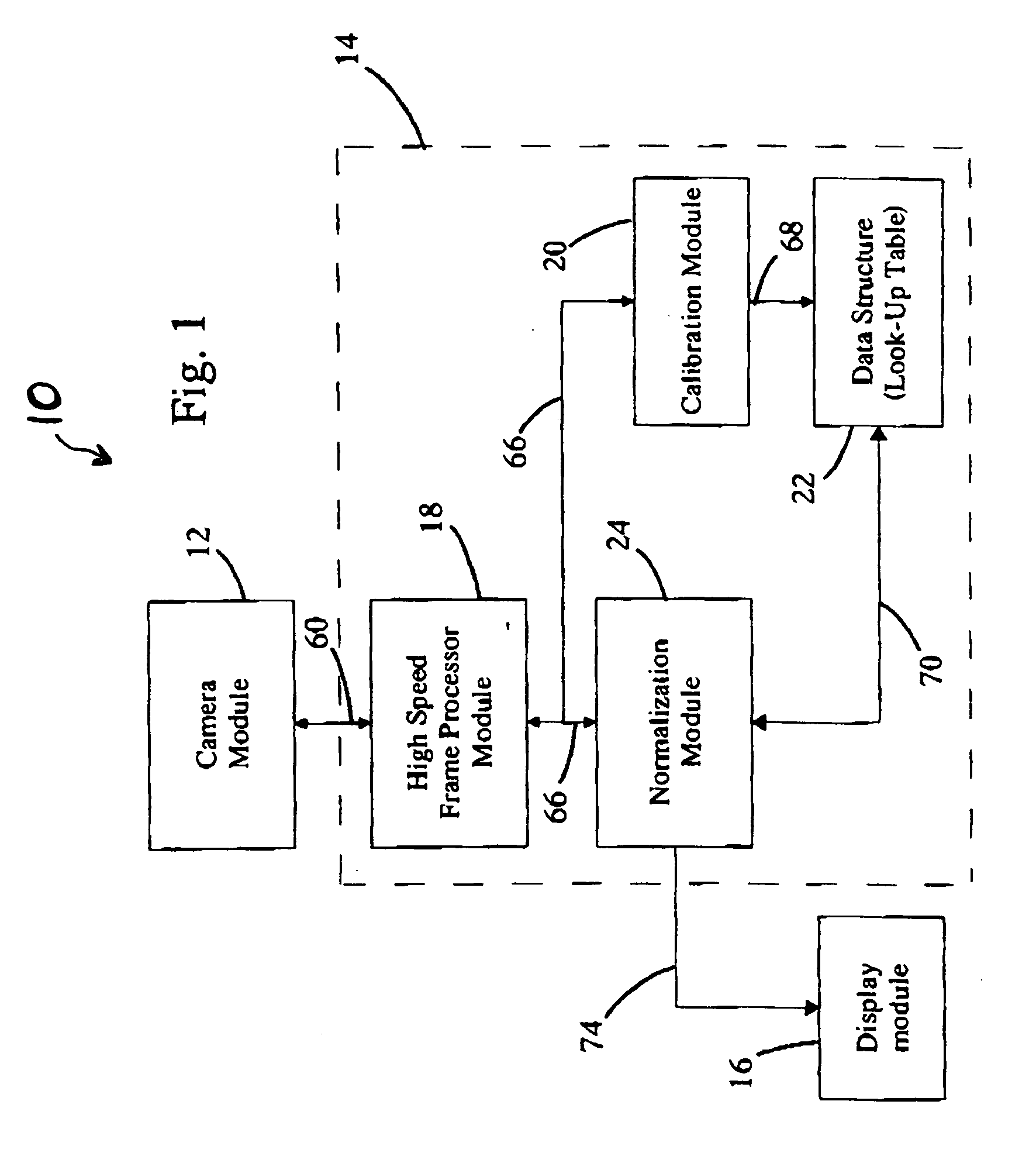
[0032] As illustrated in FIG. 1, the present invention is a high energy, real-time capable, direct radiation conversion X-ray imaging system 10. More specifically, the present invention relates to such X-ray imaging systems 10 utilizing a Cd—Te or Cd——Zn—Te based camera. The present real-time capable X-ray imaging system 10, like imaging systems generally, comprises a camera module, an image processor 14, and a display means 16. In the present real-time X-ray imaging system 10, the camera module 12 includes an X-ray imaging device 28 having a Cd—Te or Cd——Zn—Te based radiation detector substrate 30 in electrical communication with an Application Specific Integrated Circuit (ASIC...
PUM
 Abstract
Description
Claims
Application Information