Method of fabricating PCB including embedded passive chip

a technology of embedded passive chips and printed circuit boards, which is applied in the direction of printed circuit aspects, sustainable manufacturing/processing, final product manufacturing, etc., can solve the problems of reducing the interval, reducing the practicability, and avoiding the use of materials with high capacitan

Inactive Publication Date: 2006-01-19
SAMSUNG ELECTRO MECHANICS CO LTD
View PDF10 Cites 28 Cited by
  • Summary
  • Abstract
  • Description
  • Claims
  • Application Information

AI Technical Summary

Benefits of technology

[0021] Therefore, the present invention has been made keeping in mind the above disadvantages occurring in the prior arts, and an object of the present invention is to provide a method of fabricating a PCB including an embedded passive chip, in which a bli

Problems solved by technology

However, the above conventional methods are problematic in that practicality is reduced because of very low capacitance.
However, there is a difficulty in reducing the interval through the conventional methods regarding the PCB, and since material having high capacitance is very brittle, it is problematic to employ material having the high capacitance in the course o

Method used


Image

  • Method of fabricating PCB including embedded passive chip
  • Method of fabricating PCB including embedded passive chip
  • Method of fabricating PCB including embedded passive chip

Examples


first embodiment

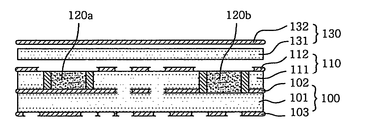
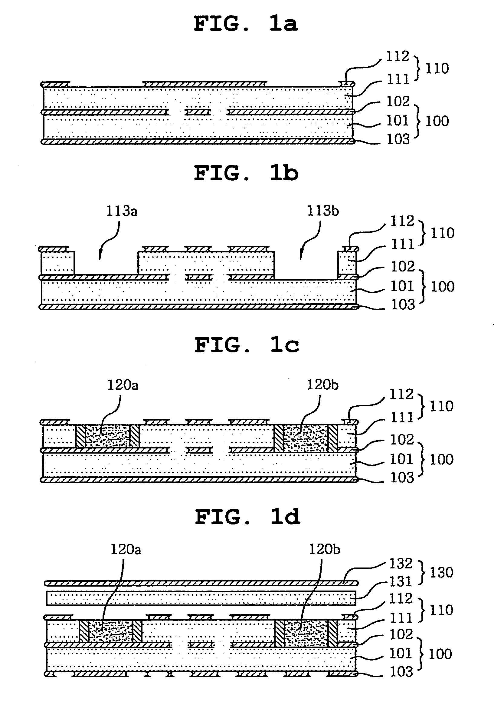
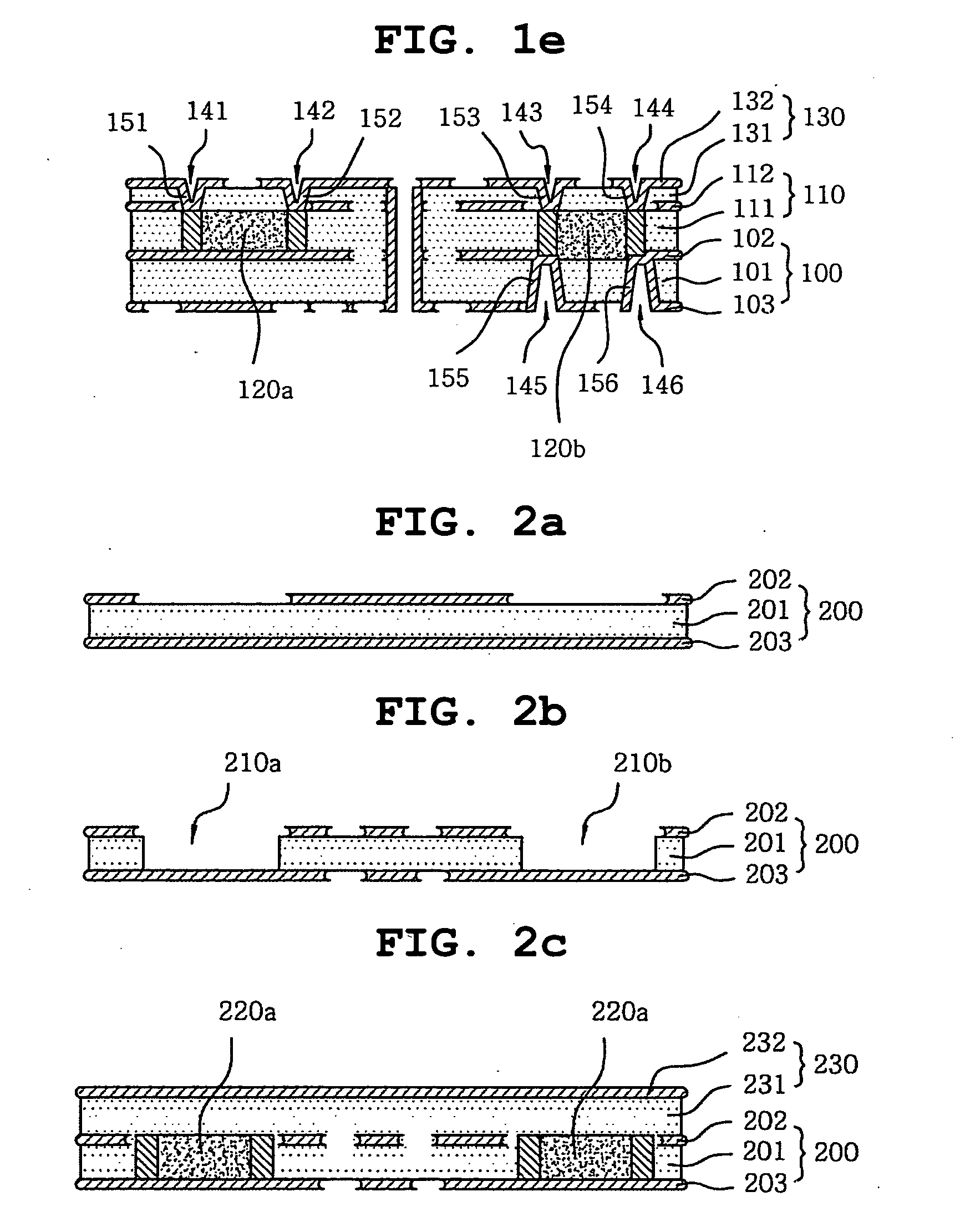
[0043]FIGS. 1a to 1e are sectional views illustrating the fabrication of a PCB including an embedded passive chip according to the present invention.

[0044] As shown in FIG. 1a, a circuit pattern is formed on a copper foil 102 of a substrate 100 constituting a core layer according to a photolithography process, and an insulator 111 or a raw material layer 110, which consists of the insulator 111 and a copper foil 112 formed on one side of the insulator 111, is laminated on the substrate 100 in a vacuum by heating and pressurization.

[0045] A copper clad laminate used as the substrate 110 may be classified into a glass / epoxy copper clad laminate, a heat-resistant resin copper clad laminate, a paper / phenol copper clad laminate, a high-frequency copper clad laminate, a flexible copper clad laminate, and a composite copper clad laminate according to its application. However, it is preferable to use the glass / epoxy copper clad laminate 100, in which copper foils 102, 103 are plated on an ...

second embodiment

[0074]FIGS. 2a to 2e are sectional views illustrating the fabrication of a PCB including an embedded passive chip according to the present invention.

[0075] The second embodiment as shown in FIGS. 2a to 2e is different from the first embodiment as shown in FIGS. 1a to 1e in that since the passive chip is mounted in a core layer, various patterns may be formed on portions of a copper foil, in which passive components are to be mounted, in the second embodiment.

[0076] As shown in FIG. 2a, copper foils 202, 203 are coated on an insulating resin layer 201 to prepare a copper clad laminate as a substrate 200, and a portion of the copper foil 202 is removed according to a photolithography process to form blind holes 210a, 210b, in which passive chips 220a, 220b are to be mounted.

[0077] Furthermore, as shown in FIG. 2b, the blind holes 210a, 210b, in which the passive chips 220a, 220b are to be mounted, are formed in the substrate 200 in such a way that the copper foil 203 positioned at b...

third embodiment

[0082]FIGS. 3a to 3d are sectional views illustrating the fabrication of a PCB including an embedded passive chip according to the present invention.

[0083] As shown in FIG. 3a, a circuit pattern is formed on a copper foil 302 of a substrate 300 constituting a core layer according to a photolithography process, and an insulator 311 or a substrate 310, which consists of the insulator 311 and a copper foil 312 formed on one side of the insulator 311, is laminated on the circuit pattern in a vacuum by heating and pressurization. In this regard, it is preferable to remove a portion of the copper foil 312, through which passive chips 320a, 320b are to be mounted, according to a photolithography process.

[0084] Subsequently, as shown in FIG. 3b, structures, in which the passive chips 320a, 320b are to be mounted, are formed according to a photolithography process, the passive chips 320a, 320b are mounted in the structures, and an insulator 341 or a substrate 340, which consists of the insu...


PUM


Abstract

Disclosed is a method of fabricating a PCB including an embedded passive chip, in which the passive chip is mounted on the PCB and an insulator is then laminated on the PCB, or in which a blind hole for receiving the passive chip is formed in the PCB and the passive chip is mounted in the blind hole.

Description

BACKGROUND OF THE INVENTION [0001] 1. Field of the Invention [0002] The present invention relates, in general, to a method of fabricating a printed circuit board (PCB) PCB including an embedded passive chip and, more particularly, to a method of fabricating a PCB including an embedded passive chip, in which a blind hole for receiving the passive chip is formed on the PCB and the passive chip is mounted in the blind hole, or in which the passive chip is mounted on the PCB and an insulator is laminated on the PCB. [0003] 2. Description of the Prior Art [0004] Typical discrete chip resistors or discrete chip capacitors have been frequently mounted on most printed circuit boards (PCB), but, recently, PCBs are developing in which passive components, such as resistors or capacitors, are embedded. [0005] A technology regarding the PCBs, including the passive components embedded therein, achieves substitution of conventional chip resistors or chip capacitors by mounting the passive componen...

Claims


Application Information

Patent Timeline
IPC IPC(8): H01L21/50
CPCH01L2224/82039H01L2924/01046H01L2924/01078H05K1/023H05K1/185H01L2924/01019H05K3/4614H05K3/4652H05K2201/10636H05K2203/1189H05K1/186Y02P70/50H05K1/16
Inventor CHO, SUK-HYEONLEE, SEOK-KYUHONG, JONG-KUKJUN, HO-SIKJEONG, JIN-SOORYU, CHANG-SUPAHN, JIN-YONG
Owner SAMSUNG ELECTRO MECHANICS CO LTD
Why Eureka
Try Eureka