Brush scrubbing-high frequency resonating substrate processing system

a processing system and high frequency technology, applied in the direction of cleaning with liquids, photosensitive materials, instruments, etc., can solve the problems of affecting the performance of integrated circuit devices, brush scrubbing operations can generally only dislodge contaminants defined on planer surfaces, and brush scrubbing operations may exhibit a rather poor cleaning capacity

Inactive Publication Date: 2006-01-26
LAM RES CORP
View PDF4 Cites 24 Cited by
  • Summary
  • Abstract
  • Description
  • Claims
  • Application Information

AI Technical Summary

Benefits of technology

[0025] The advantages of the present invention are numerous. Most notably, the embodiments of the present invention concurrently utilize brush scrubbing and high frequency acoustic energy cleaning, thus achieving a substantially improved cleaning operation. Another advantage of the present invention is that performing of brush scrubbing-AE cleaning in a single cleaning module enhances the substrate cleaning efficiency. Another advantage of the embodiments of the present invention is that by concurrently performing brush scrubbing and AE cleaning, the cleaning cycle per wafer is substantially reduced, ultimately leading to an increase in wafer throughput. Still another advantage of the present invention is that single semiconductor wafers can be cleaned substantially eliminating the possibility of recontamination of the wafer by contaminants set free during the cleaning of other semiconductor wafers. Yet another advantage of the present invention is that in the cleaning module of the present invention the cleaning operation can easily be switched between contact cleaning (brush scrubbing), non-contact cleaning (AE cleaning), or contact-noncontact cleaning, depending on the application requirements. Yet another advantage is that the embodiments of the present invention can be implemented in a multi-station cleaning module designed to clean a plurality of substrates in individual combination cleaning modules.

Problems solved by technology

It is well established that contaminants should be removed as the presence of such contaminants has detrimental effects on the performance of the integrated circuit devices.
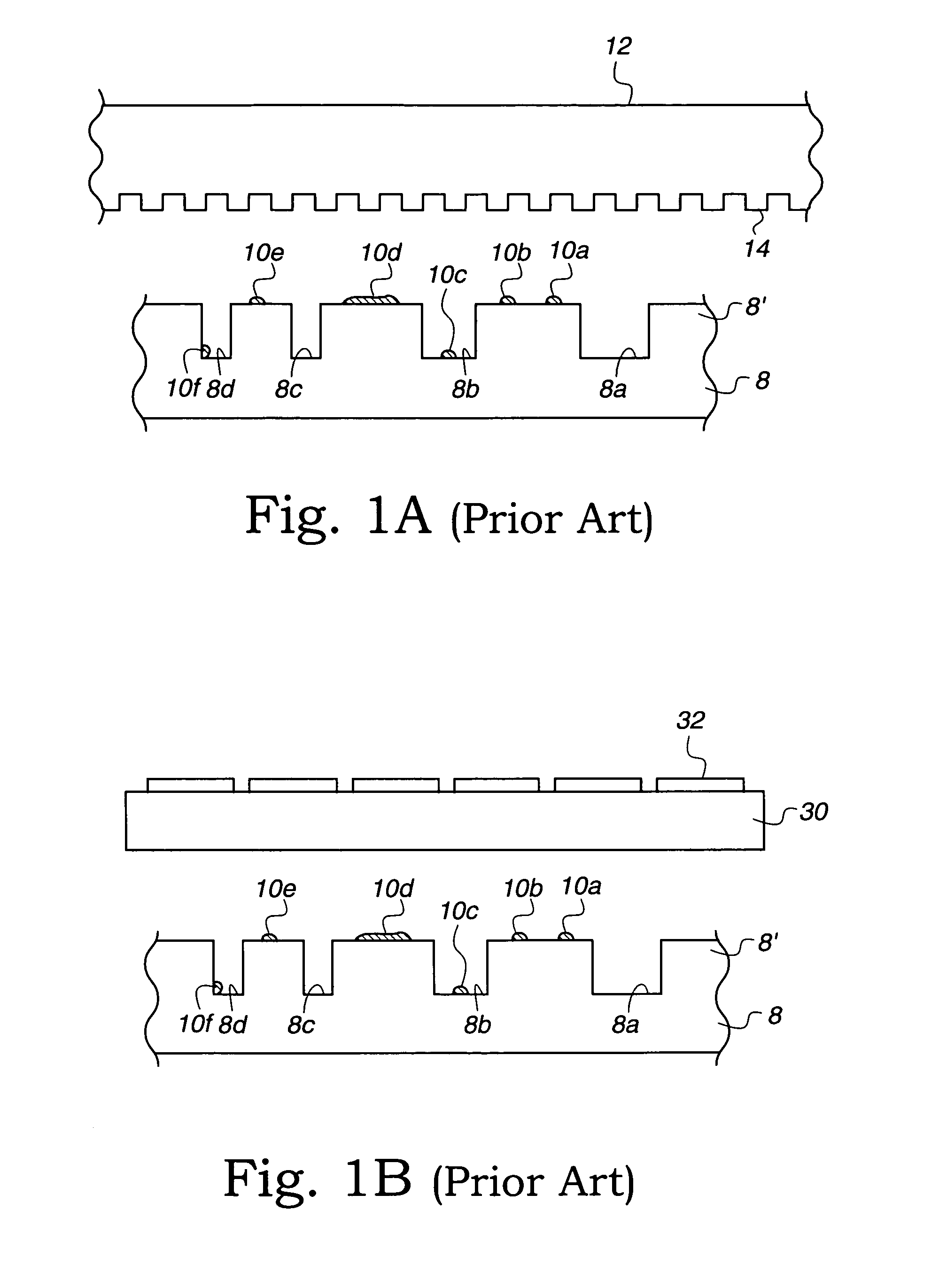
Unfortunately, brush scrubbing operations can generally only dislodge contaminants defined on planer surfaces, i.e., 10a, 10b, 10d, and 10e.
As a result, brush scrubbing operations may exhibit a rather poor cleaning capacity when cleaning surface topography features such as trenches or vias open to the wafer surface 8′.
In some circumstance, this limitation associated with brush scrubbing operations becomes more noticeable as the feature sizes get smaller (e.g., smaller than 0.2 microns).
As can be appreciated, smaller feature sizes may prevent penetration of the brush material into the topography features, thus limiting or blocking access to the contaminants lodged therein.
However, megasonic cleaning may achieve an inadequate cleaning of the planer surfaces.
Furthermore, as shown, megasonic cleaning may not be capable of dislodging contaminants pressed onto the wafer surface 8′, such as contaminant 10d.
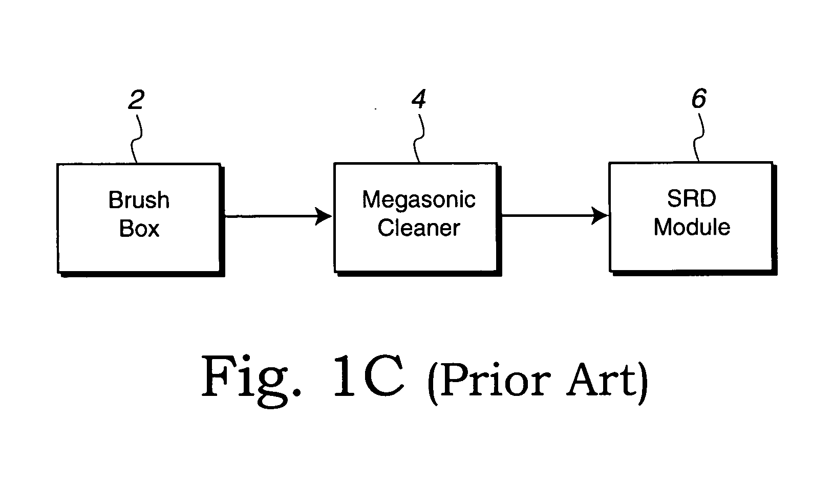
In this manner, the cleaning cycle for each wafer is significantly and unnecessarily increased.
As can be appreciated, this reduces the overall wafer throughput.

Method used


Image

  • Brush scrubbing-high frequency resonating substrate processing system
  • Brush scrubbing-high frequency resonating substrate processing system
  • Brush scrubbing-high frequency resonating substrate processing system

Examples


Embodiment Construction

[0048] Several exemplary embodiments of the invention will now be described in detail with reference to the accompanying drawings. FIGS. 1A, 1B, and 1C are discussed above in the “Background of the Invention” section.

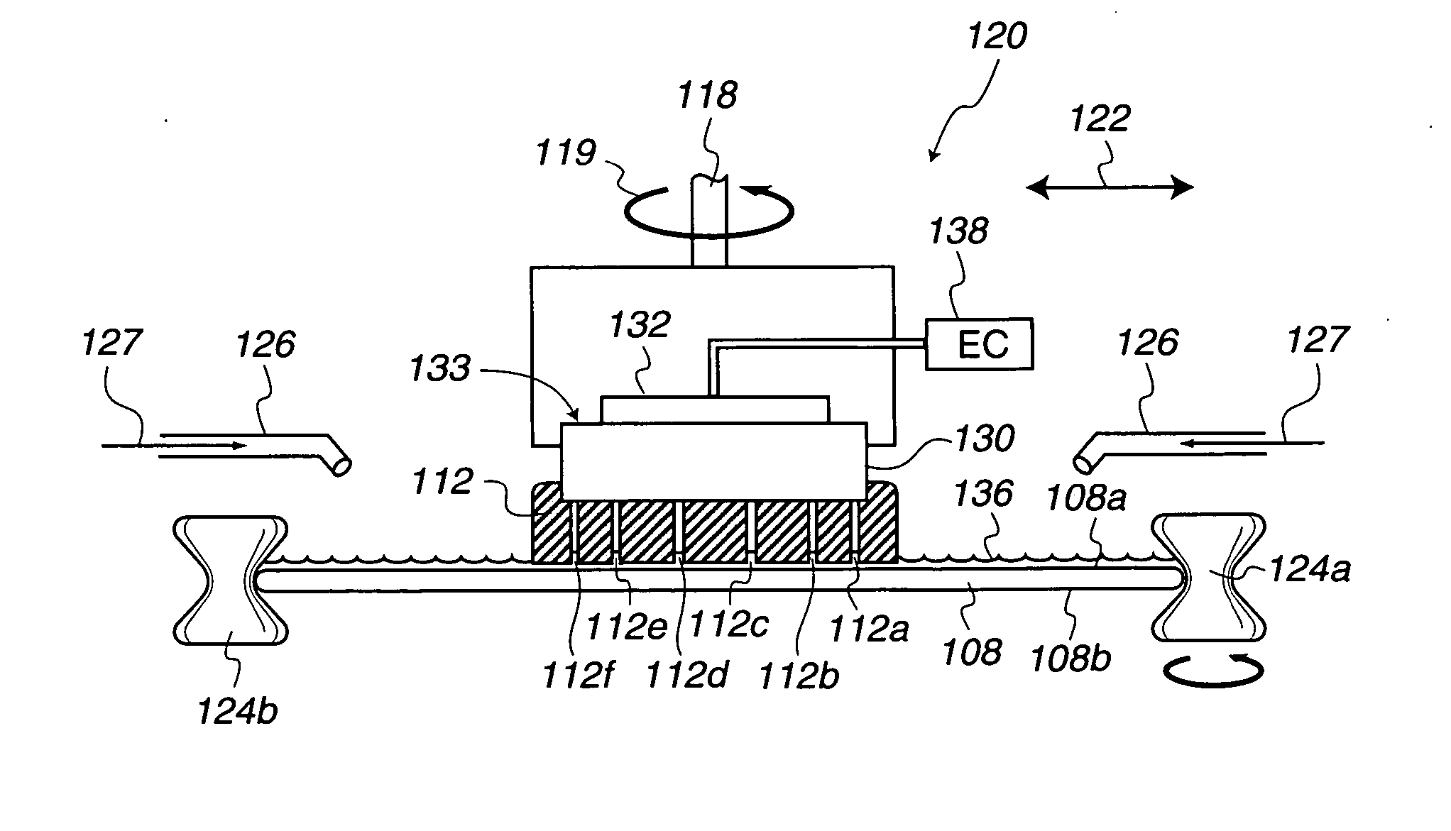
[0049] The embodiments of the present invention provide an apparatus and a method for cleaning a semiconductor substrate by concurrently using a combination of high frequency acoustic energy cleaning and brush scrubbing in a stand alone cleaning module. In one embodiment, a brush scrubbing-high frequency acoustic energy cleaning assembly capable of substantially removing contaminants lodged on wafer planer surfaces or deep wafer topography features. In one embodiment, a flat brush scrubbing-acoustic energy (AE) cleaning assembly is provided. The flat brush scrubbing-AE cleaning assembly is includes a housing, a transducer having a crystal bonded to a resonator, and an arm configured to move the housing and thus the flat brush scrubbing-AE cleaning assembly. A flat brus...


PUM


Abstract

A substrate processing system is provided. The substrate processing system comprises a brush assembly that includes a core, a transducer, and a brush. The core is configured to include a plurality of orifices extending from a center of the brush core to an outer surface of the brush core. The transducer is configured to be disposed on an outer surface of the core. The transducer is capable of resonating at a high frequency. The brush includes a plurality of openings, and is configured to cover the transducer. When the transducer resonates at the high frequency, high energy acoustic energy is imparted from the transducer to a surface of a substrate to be prepared at a respective location of each opening of the plurality of openings.

Description

CROSS-REFERENCE TO RELATED APPLICATION [0001] This Application is a Divisional of Application No. 10 / 377,944, filed on Feb. 28, 2003, from which priority under 35 U.S.C. § 120 is claimed. The disclosure of this Application is incorporated herein by reference.BACKGROUND OF THE INVENTION [0002] 1. Field of the Invention [0003] The present invention relates generally to substrate surface cleaning and, more particularly, to a method and apparatus for improving semiconductor substrate cleaning following fabrication processes. [0004] 2. Description of the Related Art [0005] As is well known to those skilled in the art, the fabrication of semiconductor devices involves numerous processing operations. These operations include, for example, impurity implants, gate oxide generation, inter-metal oxide depositions, metallization depositions, photolithography patterning, etching operations, chemical mechanical polishing (CMP), etc. Typically, these operations generate contaminants such as partic...

Claims


Application Information

Patent Timeline
Patent Type & Authority Applications(United States)
IPC IPC(8): B08B3/12A47L25/00B08B1/04B08B3/00H01L21/00
CPCB08B1/04H01L21/67046B08B3/12
Inventor MIKHAYLICHENKO, KATRINAREDEKER, FRITZ C.
Owner LAM RES CORP
Why Eureka
Try Eureka