CMOS active pixel sensor with improved dark current and sensitivity

a technology of active pixel sensor and dark current, which is applied in the field can solve the problems of dark current and sensitivity of active pixel sensor fabricated using standard cmos processing, and achieve the effect of improving the sensitivity of active pixel sensor and reducing the dark curren

Active Publication Date: 2006-01-26
GULA CONSULTING LLC
View PDF12 Cites 12 Cited by
  • Summary
  • Abstract
  • Description
  • Claims
  • Application Information

AI Technical Summary

Benefits of technology

[0014] The gate electrode is biased so that the region of the substrate under the gate electrode is accumulated with electrons and the region of the P well under the gate electrode is depleted of holes. This will

Problems solved by technology

However, active pixel sensors fabricated using standard CMOS processing have a problem with

Method used


Image

  • CMOS active pixel sensor with improved dark current and sensitivity
  • CMOS active pixel sensor with improved dark current and sensitivity
  • CMOS active pixel sensor with improved dark current and sensitivity

Examples


Embodiment Construction

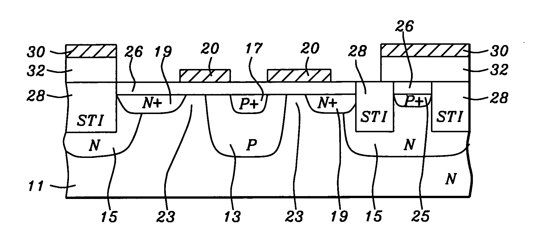
[0019] Refer now to FIGS. 1 and 2 for a detailed description of a preferred embodiment of this invention. FIG. 1 shows a cross section view of the pixel of this embodiment and FIG. 2 a top view. In this embodiment an N well 12 is formed in a substrate 10 of P type epitaxial silicon. A P well 14 is also formed in the substrate 10 of P type epitaxial silicon and surrounds the N well 12 as can be seen in FIG. 2. The N well 12 is N type silicon and the P well 14 is P type silicon. A first N+ region 16 can be formed in the N well 12 and can be used to make electrical contact to the N well 12. A second N+ region 24, which is not essential to the invention, can be formed in the P well 14. Active devices can be formed in the P well using the second N+ region 24. A P+ region 18 is formed in part of the P well 14 and part of the substrate 10 and surrounds the N well 12 leaving a gap 22 between the inner periphery of the P+ region 18 and the N well 12.

[0020] The P well 14 can provide isolatio...


PUM


Abstract

An active pixel sensor which provides reduced dark current, improved sensitivity, and improved modulation transfer function. An N well, surrounded by a P well is formed in a P type epitaxial substrate. A P+ region is formed extending from within the P well into the substrate leaving a gap between the P+ region and the N well. A gate dielectric is formed covering at least the gap, part of the P+ region, and part of the N well. A gate electrode is formed on the gate dielectric over the gap, part of the P+ region, and part of the N well. The gate electrode is biased so that the region of the substrate under the gate electrode is accumulated with holes and the region of the N well under the gate electrode is depleted of electrons. This will reduce the dark current and improve the sensitivity of the active pixel sensor. In a second embodiment the P type epitaxial substrate is replaced by an N type epitaxial substrate, the N well is replaced by a P well, N+ regions are replaced by P+ regions, and P+ regions are replaced by N+ regions. In this second embodiment the gate electrode is biased so that the region of the substrate under the gate electrode is depleted of electrons and the region of the P well under the gate electrode is accumulated with holes.

Description

[0001] This Patent Application claims priority to the following U.S. Provisional Patent Application, herein incorporated by reference: [0002] 60 / 590,406, filed Jul. 22, 2004.BACKGROUND OF THE INVENTION [0003] (1) Field of the Invention [0004] This invention relates to an active pixel sensor fabricated using standard CMOS processing and more particularly to dark current suppression and improved sensitivity in active pixel sensors fabricated using standard CMOS processing. [0005] (2) Description of the Related Art [0006] U.S. Pat. No. 6,649,950 B2 to He et al. describes substantially covering the surface of a photodiode structure in order to reduce dark current due to surface damage to the photodiode structure. [0007] U.S. Pat. No. 6,621,064 B2 to Chen et al. describes a device utilizing a buried junction away from the surface to reduce dark current. [0008] U.S. Patent Application Publication No. US 2004 / 0046104 A1 by Rhodes describes a CMOS imager in which the floating diffusion is c...

Claims


Application Information

Patent Timeline
IPC IPC(8): H01L29/94H01L31/113H01L27/148H01L29/768H01L31/06
CPCH01L27/14603H01L27/14643H01L27/1463H01L27/14609
Inventor DOSLUOGLU, TANER
Owner GULA CONSULTING LLC
Why Eureka
Try Eureka