BGA package board and method for manufacturing the same

Active Publication Date: 2006-01-26
SAMSUNG ELECTRO MECHANICS CO LTD
View PDF5 Cites 32 Cited by
  • Summary
  • Abstract
  • Description
  • Claims
  • Application Information

AI Technical Summary

Benefits of technology

[0023] Accordingly, the present invention has been made keeping in mind the above problems occurring in the prior art, and an object of the p

Problems solved by technology

Particularly, such adhesion of the solder balls 19 may occur more frequently when the BGA pa

Method used


Image

  • BGA package board and method for manufacturing the same
  • BGA package board and method for manufacturing the same
  • BGA package board and method for manufacturing the same

Examples


Example

[0041] Hereinafter, a Ball Grid Array (BGA) package board and a manufacturing method thereof according to the present invention will be described in detail with reference to the attached drawings.

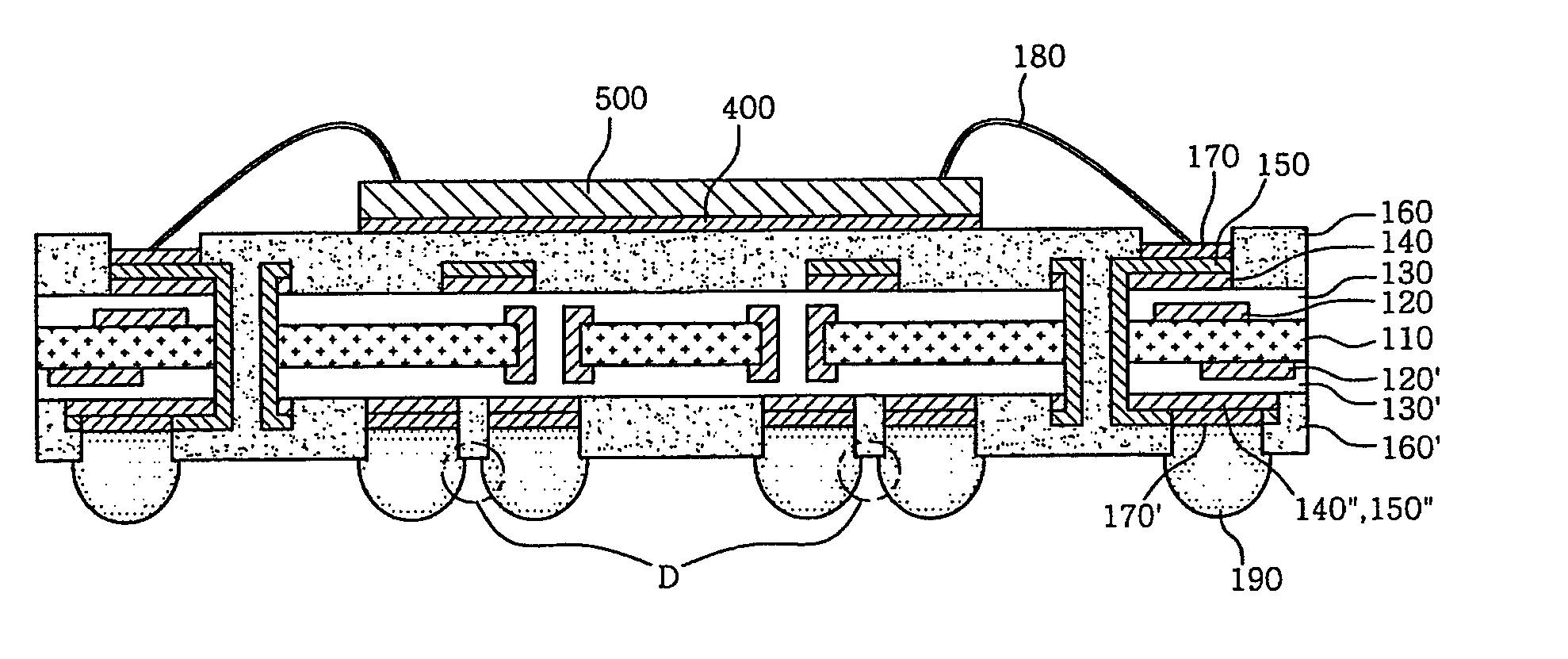
[0042]FIGS. 3a to 3o are sectional views to show a method for manufacturing a BGA package board, according to an embodiment of the present invention, and FIG. 4 is a sectional view of a CSP (Chip-Sized Package) with a semiconductor chip mounted on the BGA package board manufactured through the method of FIGS. 3a to 3o.

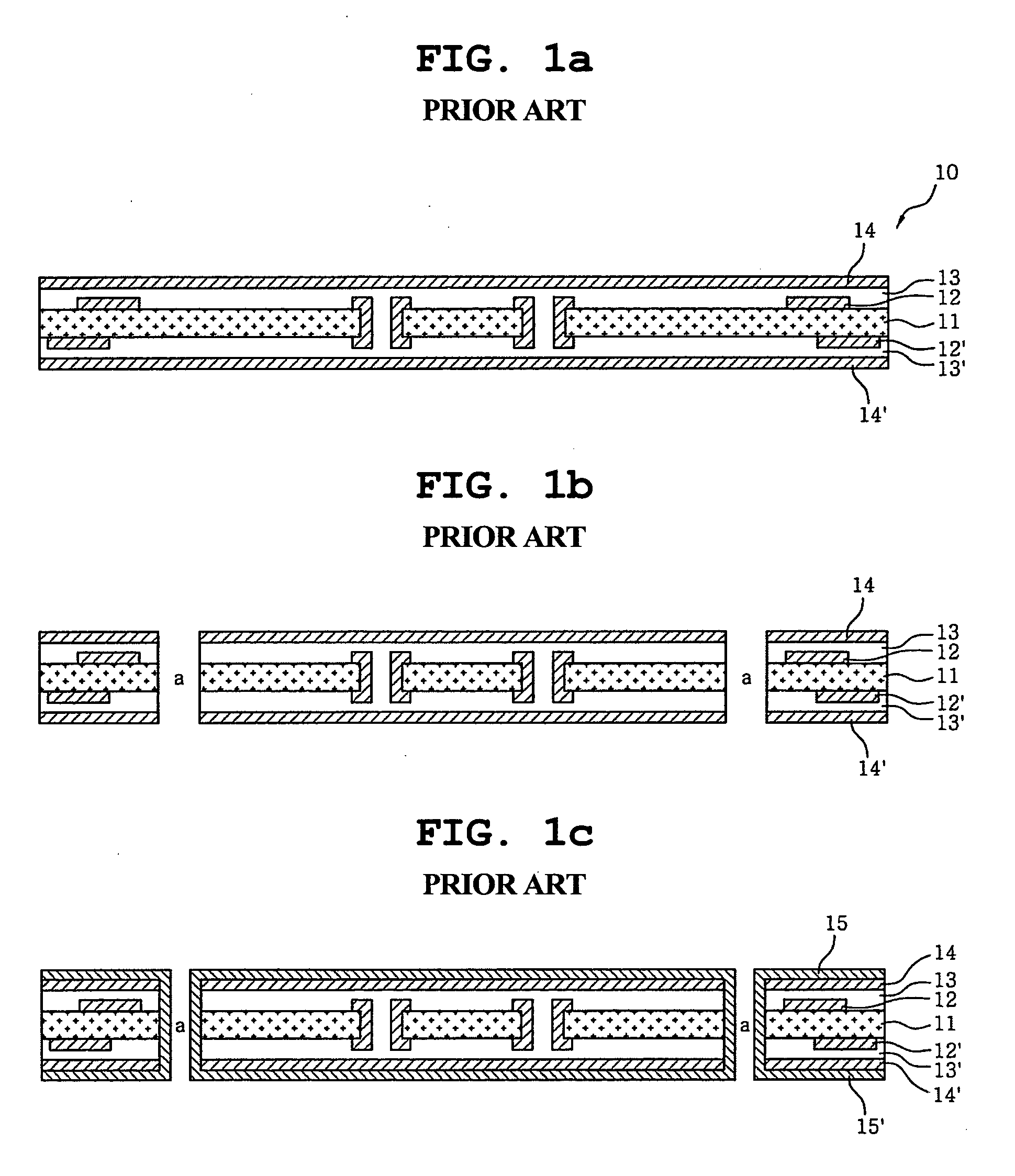
[0043] As shown in FIG. 3a, a base plate 100 is prepared, which is constructed as follows. The base plate 100 includes a copper clad laminate having an insulating resin layer 110 and copper foil layers 120 and 120′ on which circuit patterns are formed. Further, insulating layers 130 and 130′, for example, prepreg, and copper foils 140, 140′ are laminated on both surfaces of the copper clad laminate.

[0044] In this case, the copper clad laminate used as an internal layer of t...


PUM


Abstract

Disclosed herein is a Ball Grid Array (BGA) package board. The BGA package board includes a first external layer on which a pattern comprising a circuit pattern and a wire bonding pad pattern is formed, a second external layer on which a pattern comprising a circuit pattern and a solder ball pad pattern is formed, an insulating layer formed between the first and second external layers, a first outer via hole to electrically connect the first and second external layers to each other, and a solder resist layer formed on each of the first and second external layers, with portions of the solder resist layer corresponding to the wire bonding pad pattern and the solder ball pad pattern being opened. The solder ball pad pattern is thinner than the circuit pattern of the second external layer.

Description

BACKGROUND OF THE INVENTION [0001] 1. Field of the Invention [0002] The present invention relates generally to a BGA (Ball Grid Array) package board and a manufacturing method thereof, and more particularly, to a BGA package board and a manufacturing method thereof, capable of preventing solder balls from adhering to each other by adjusting the thickness of a solder ball pad. [0003] 2. Description of the Related Art [0004] Recently, as miniaturization and higher integration of multi-functional electronic devices are achieved, BGA package board technology has been rapidly developed to realize lightness, thinness, shortness, and smallness and a fine circuit pattern of a high density. Particularly, the lightness, thinness, shortness, and smallness and the fine circuit pattern have been increasingly required for a CSP (Chip-Sized Package) with a semiconductor chip mounted on the BGA package board. [0005]FIG. 1a to 1k are sectional views to show a method for manufacturing a conventional ...

Claims


Application Information

Patent Timeline
IPC IPC(8): H01L23/12H01L21/50
CPCH01L21/4853H01L23/49816H01L23/49822H01L23/49838H01L24/48H01L2224/0401H01L2224/05155H01L2224/05599H01L2224/05644H01L2224/05647H01L2224/32225H01L2224/48091H01L2224/48227H01L2224/48228H01L2224/484H01L2224/73265H01L2224/85444H01L2924/01004H01L2924/01005H01L2924/01006H01L2924/01011H01L2924/01013H01L2924/01028H01L2924/01029H01L2924/01046H01L2924/0105H01L2924/01078H01L2924/01079H01L2924/014H01L2924/15311H05K3/061H05K3/243H05K3/28H05K3/427H05K3/429H05K3/4652H05K2201/0352H05K2201/09536H05K2201/09736H05K2203/0353H05K2203/0574H05K2203/0577H01L2924/00014H01L2924/01019H01L2924/01033Y10T29/4913Y10T29/49135Y10T29/49147Y10T29/49165Y10T29/49155Y10T29/49128H01L2224/45099H01L2924/00H01L2924/00012H01L24/73H01L21/60
Inventor YOON, KYOUNG-ROSHIN, YOUNG-HWANLEE, TAE-GON
Owner SAMSUNG ELECTRO MECHANICS CO LTD
Why Eureka
Try Eureka