
Common-mode shifting circuit for CML buffers

a common-mode switching and buffer technology, applied in logic circuit coupling/interface arrangement, digital transmission, pulse technique, etc., can solve the problems of limiting headroom or voltage swing, insensitive to common-mode noise, negatively affecting ac output signals, etc., to reduce common-mode voltage, lower common-mode voltage, and lower common-mode voltage

Inactive Publication Date: 2006-01-26
AVAGO TECH WIRELESS IP SINGAPORE PTE
View PDF9 Cites 8 Cited by
  • Summary
  • Abstract
  • Description
  • Claims
  • Application Information

AI Technical Summary

Benefits of technology

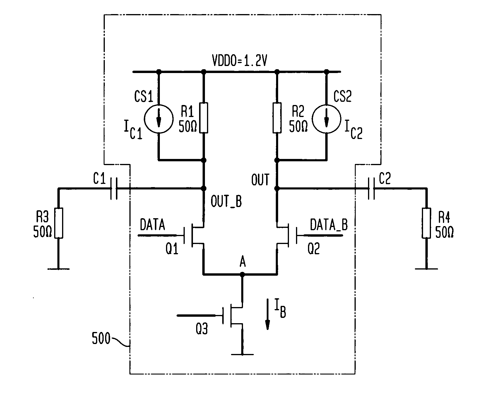
[0013] Briefly described, the invention is a current-mode level-shifting circuit that can shift the common-mode output voltage of a CML device to an arbitrary voltage, preferably close to the voltage of the power supply rails. The circuit provides a common-mode output voltage that is well-suited for operation with low-voltage power supplies. In accordance with the invention, a constant current is provided at each output, respectively, of the CML device via a constant current source. If the constant current at each output is a positive current flowing into the output, the common-mode output voltage will be raised. Alternatively, if the constant current at each output is a negative current flowing out from the output, the common-mode voltage will be lowered. Preferably, the constant currents provided at the outputs are approximately the same. The constant current sources may be implemented as PMOS transistors biased to a condition sufficient to provide a current adequate to raise the common-mode voltage.
[0014] Thus, the invention may broadly be described as a current-mode shifting circuit, comprising a current-mode logic circuit having two input ports and two output ports having a common-mode voltage; and two constant-current sources, each connected respectively between the two output ports of said current-mode logic circuit and a first supply voltage. The constant-current sources produce currents at the output ports that shift the common-mode voltage at the output ports. In one embodiment, the first supply voltage is greater than the common-mode voltage at the output ports, such the constant current sources inject current into the output ports and thereby raise the common-mode voltage. Alternatively, the first supply voltage may be less than the common-mode voltage at the output ports, such that the constant current sources sink current from the output ports and thereby lower the common-mode voltage. The current-mode shifting circuit may further comprise two DC block capacitors, each connected respectively to the two output ports of the current-mode logic circuit, and capable of connection to a load termination.
[0015] In a further embodiment, the current-mode logic circuit is connected to a second supply voltage. Preferably, the first supply voltage (connected to the current sources) is equal to or greater than the second supply (connected to the current-mode logic circuit). The constant-current sources may then inject sufficient current into the output ports to raise the common-mode voltage at each output port to a sufficiently high value that the peak voltage at each output port of the current-mode logic circuit is greater than the first power supply voltage. It may still further include load resistors connected between the current sources and the output ports of the current-mode logic circuit. In this embodiment, it is also preferable to provide two resistors connected in series with the current sources. These resistors act as current-limiting resistors and buffer the current sources from output fluctuations.
[0016] The invention further provides a method for adjusting the output signal of a current-mode logic circuit having two output ports and connected to a first supply voltage. The method comprises the step of providing a constant current at each output of the current-mode logic circuit, whereby the common-mode voltage at the output ports of the current-mode logic circuit is level-shifted. The constant current may be a negative current flowing out of each output port, thus lowering the common-mode voltage, or may be a positive current flowing into each output port, thus raising the common-mode voltage. In this latter embodiment, the constant current injected at each output port preferably raises the common-mode voltage to a sufficiently high value that the peak voltage at each output port of the current-mode logic circuit is greater than the first power supply voltage. The method preferably also includes passing the constant current at each output port through a series resistor.

Problems solved by technology

Further, because CML buffers use differential signaling, they are relatively insensitive to common-mode noise.
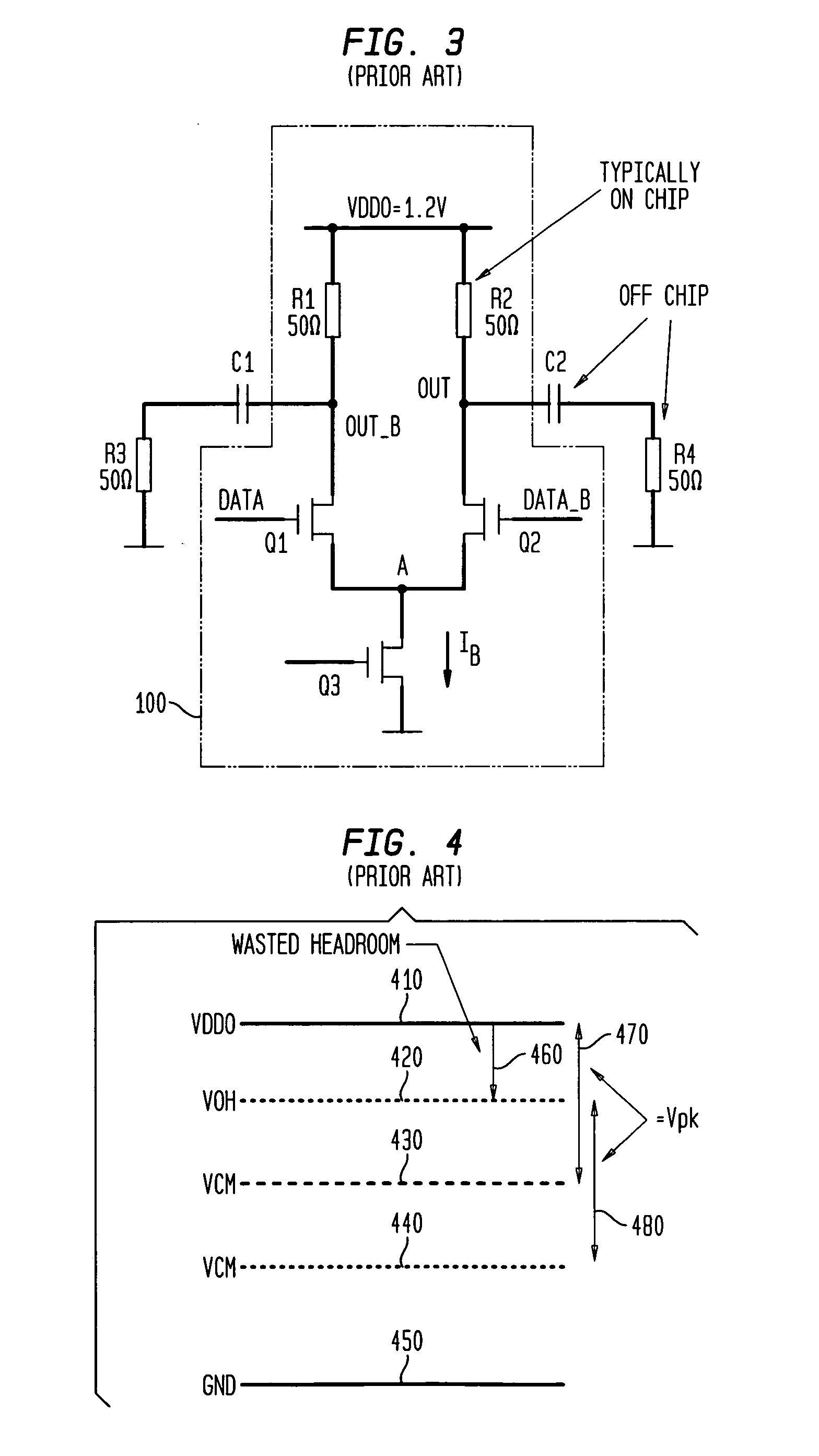
A significant problem arises, however, when a CML buffer is connected to a receiver through a DC blocking capacitor (known as “AC coupling mode”).
The large downward shift in the common-mode voltage VCM negatively impacts the AC output signal, however, by limiting the headroom or voltage swing that is available.
As a result, at low power supply voltages (for example, 1.2 volts or less), “clipping” or distortion of the output signal may occur.
The very low level of the minimum output voltage VOL (0.45 V), however, causes these transistors to tend to operate in active or cut-off mode, causing distortion or clipping.
In practice, however, the benefit of a high W / L ratio must be balanced against the parasitic capacitance of the devices, which increases as the W / L ratio increases and which tends to reduce the switching frequency of the devices.

Method used


Image

  • Common-mode shifting circuit for CML buffers
  • Common-mode shifting circuit for CML buffers
  • Common-mode shifting circuit for CML buffers

Examples


Embodiment Construction

[0027] A current-mode shifting circuit in accordance with the present invention is shown in FIG. 5. Similarly to CML buffer 100 described above, current-mode shifting circuit 500, includes two local (on-chip) 50-ohm resistors R1 and R2, two input transistors Q1 and Q2, and a “tail current” transistor Q3. Resistors R1 and R2 are connected between supply voltage VDDO and the current-supply (or “drain”) terminals of transistors Q1 and Q2, respectively. The current-sink (or “source”) terminals of transistors Q1 and Q2 are connected together at node A to the current-supply terminal of transistor Q3. The current-sink terminal of transistor Q3 is connected to ground. In accordance with one embodiment of the invention, current-mode shifting circuit 500 further includes two constant-current sources CS1 and CS2, each connected respectively to the two outputs OUT_B and OUT of current-mode logic circuit 500.

[0028] Like CML buffer 100 described above, current-mode shifting circuit 500 receives ...


PUM


Abstract

A common-mode shifting circuit for shifting the common-mode output voltage of a CML device to an arbitrary voltage is disclosed. A constant current source is provided at each output of the CML device. The constant current may be a positive or negative current, tending to raise or lower the common-mode output voltage, respectively. The constant current sources are preferably connected to an alternate voltage supply having a higher voltage than that the supply for the CML device. The invention further provides a method for adjusting the output signal of a current-mode logic circuit having two or more output ports, comprising the step of providing a constant current at each output port of the current-mode logic circuit, whereby the common-mode voltage at the output ports of said current-mode logic circuit is level-shifted.

Description

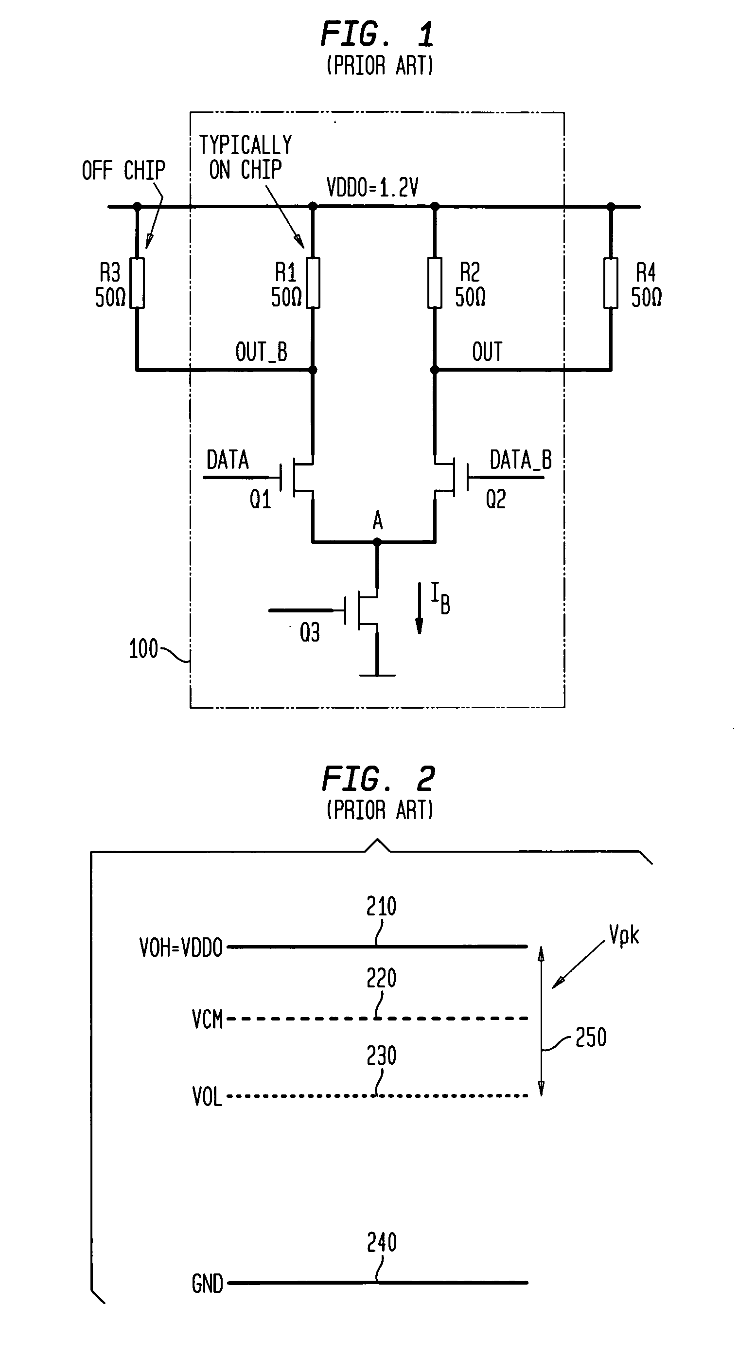
CROSS-REFERENCES [0001] This application claims the benefit of U.S. Provisional Application No. 60 / 590,624, filed Jul. 23, 2004.FIELD OF THE INVENTION [0002] The present invention relates generally to signal levels in current-mode logic circuits, especially in high-speed input / output interface circuits. BACKGROUND OF THE INVENTION [0003] In high-speed communications equipment, e.g., optical transceivers or high-speed input-output (I / O) interface circuits, current-mode logic (“CML”) buffers are frequently employed to drive off-chip resistive loads. CML buffers generally are able to operate from relatively low power supplies and achieve very fast switching high speeds, e.g., greater than a gigahertz or several tens of gigahertz. Further, because CML buffers use differential signaling, they are relatively insensitive to common-mode noise. [0004] A conventional CML buffer circuit is shown in FIG. 1. CML buffer 100 includes two local (on-chip) 50-ohm resistors R1 and R2, two input transi...

Claims


Application Information

Patent Timeline
Patent Type & Authority Applications(United States)
IPC IPC(8): H03K19/094
CPCH03K19/09432H04L25/0282H04L25/0274H03K19/0175
Inventor AZADET, KAMERANYANG, FUJIGUO, CHUNBING
Owner AVAGO TECH WIRELESS IP SINGAPORE PTE
Learn More