Transistor fabrication methods using dual sidewall spacers

a fabrication method and transistor technology, applied in the direction of transistors, semiconductor devices, electrical equipment, etc., can solve the problems of high cost of additional alloy layers and silicon layers, significant impact on power consumption and switching performance, etc., to facilitate inducing enhanced stress in the transistor channel, improve source/drain contact resistance, and improve the effect of pmd gap fill

Active Publication Date: 2006-01-26
TEXAS INSTR INC
View PDF18 Cites 254 Cited by
  • Summary
  • Abstract
  • Description
  • Claims
  • Application Information

AI Technical Summary

Benefits of technology

[0006] The invention relates to methods for transistor fabrication, in which relatively wide sidewall spacers are provided along lateral sides of a transistor gate structure during deep source/drain implantation to control the location of the source/drains on either side of the transistor channel region, and the spacers are narrowed after the deep source/drain implant to facilitate inducing enhanced stress in the transistor channel, to improve source/drain contact resistance, and to improve PMD gap fill. The invention may be employed in conjunction with stress inducing PMD liner material layers formed over the transistor after source/drain implantation, wherein the reduced sidewall spacer width facilitates inducing enhanced stress at the center of the transistor channel.
[0007] In accordance with one aspect of the invention, a method is provided for fabricating a transistor. The method comprises forming a gate structure, forming a first sidewall spacer along

Problems solved by technology

Carrier mobility in a MOS transistor has a significant impact on power consumption and switching performance.
However, buried silicon/germanium channel layer devices have shortcomings, including increased alloy scattering in the channel region that degrades electron mobility, a lack of favorable conducti

Method used


Image

  • Transistor fabrication methods using dual sidewall spacers
  • Transistor fabrication methods using dual sidewall spacers
  • Transistor fabrication methods using dual sidewall spacers

Examples


Embodiment Construction

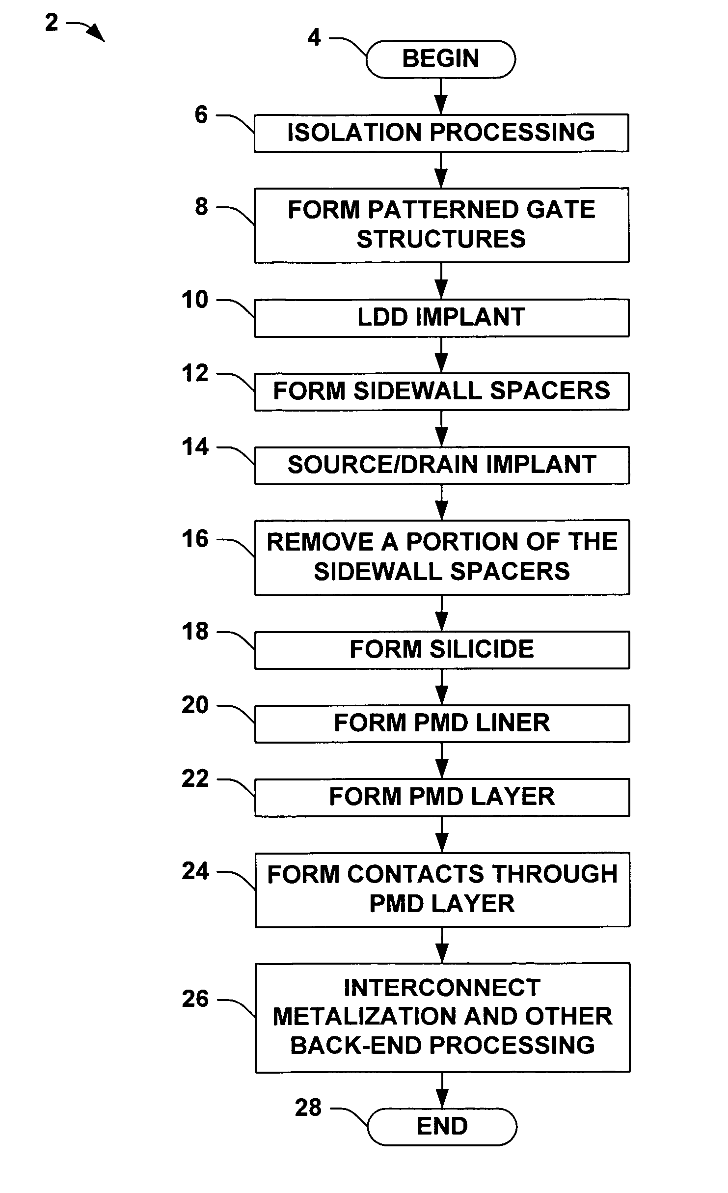
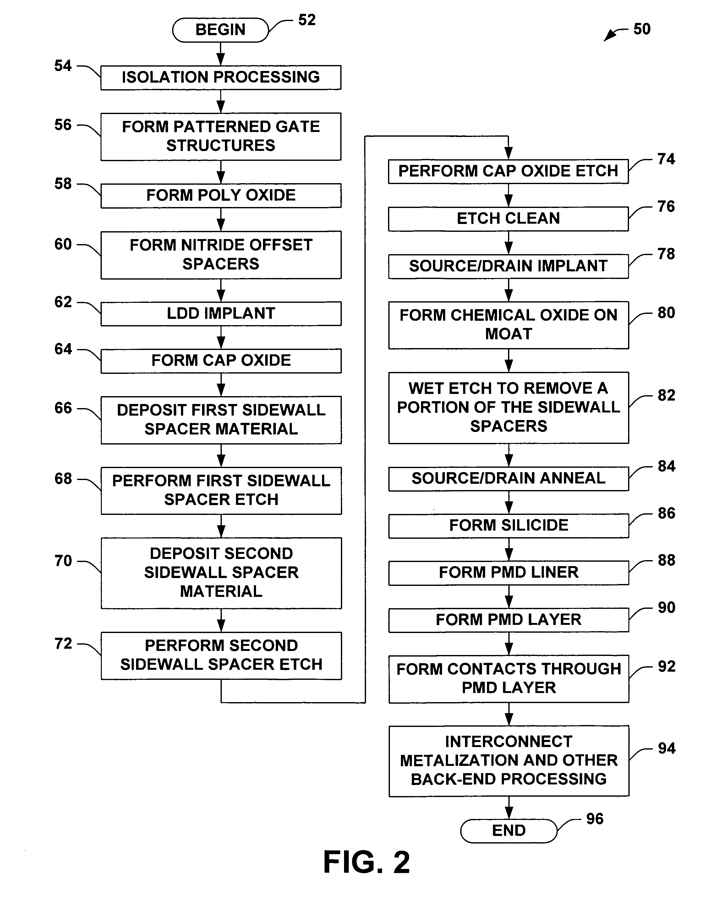
[0012] One or more implementations of the present invention will now be described with reference to the attached drawings, wherein like reference numerals are used to refer to like elements throughout, and wherein the illustrated structures are not necessarily drawn to scale.

[0013] The invention provides techniques for improving transistor performance by facilitating application of stress to improve carrier mobility, such as tensile stress provided to NMOS channel regions, and by source / drain contact resistance improvement. In one particular implementation illustrated and described hereinafter, a stress inducing PMD liner nitride film is formed over the transistor following silicide processing to impart stress in the transistors, where the liner protects the underlying transistors from a subsequently formed pre-metal dielectric (PMD) material and operates as an etch-stop layer in forming openings for contacts to transistor terminals through the PMD material. In accordance with the ...


PUM


Abstract

Methods (50) are presented for transistor fabrication, in which first and second sidewall spacers (120a, 120b) are formed laterally outward from a gate structure (114), after which a source/drain region (116) is implanted. The method (50) further comprises removing all or a portion of the second sidewall spacer (120b) after implanting the source/drain region (116), where the remaining sidewall spacer (120a) is narrower following the source/drain implant to improve source/drain contact resistance and PMD gap fill, and to facilitate inducing stress in the transistor channel.

Description

FIELD OF INVENTION [0001] The present invention relates generally to semiconductor devices and methods for making the same. BACKGROUND OF THE INVENTION [0002] Current trends in the semiconductor industry include faster switching speeds, reduced power consumption, and lower operating voltages, wherein the performance of MOS transistors needs to be correspondingly improved. For example, high-speed transistors are required for modern wireless communications systems, portable computers, and other low-power, low-voltage devices, wherein MOS transistors must be adapted to operate at lower voltages using less power. Carrier mobility in a MOS transistor has a significant impact on power consumption and switching performance. The carrier mobility is a measure of the average speed of a carrier (e.g., holes or electrons) in a given semiconductor, given by the average drift velocity of the carrier per unit electric field. Improving the carrier mobility in the channel region of a MOS transistor ...

Claims


Application Information

Patent Timeline
IPC IPC(8): H01L21/336
CPCH01L29/665H01L29/6653H01L29/6656H01L29/7843H01L29/7833H01L29/7842H01L29/6659
Inventor BU, HAOWENCHIDAMBARAM, PRKHAMANKAR, RAJESHHALL, LINDSEY
Owner TEXAS INSTR INC
Why Eureka
Try Eureka