Directionally controlled growth of nanowhiskers

a nanowhisker and growth technology, applied in the direction of crystal growth process, physical/chemical process catalyst, metal/metal-oxide/metal-hydroxide catalyst, etc., can solve the problem of high density of stacking faults that commonly form, defects are expected to affect the physical properties of nanowhiskers, and the main surface of (001) substrates commonly used in industrial applications. problems, to achieve the effect of reducing the amount of constituent materials, well-defined surface, and fast growth

a nanowhisker and growth technology, applied in the direction of crystal growth process, physical/chemical process catalyst, metal/metal-oxide/metal-hydroxide catalyst, etc., can solve the problem of high density of stacking faults that commonly form, defects are expected to affect the physical properties of nanowhiskers, and the main surface of (001) substrates commonly used in industrial applications. problems, to achieve the effect of reducing the amount of constituent materials, well-defined surface, and fast growth

US20060019470A1Inactive Publication Date: 2006-01-26QUNANO

Image

  • Directionally controlled growth of nanowhiskers
  • Directionally controlled growth of nanowhiskers
  • Directionally controlled growth of nanowhiskers

Examples


Embodiment Construction

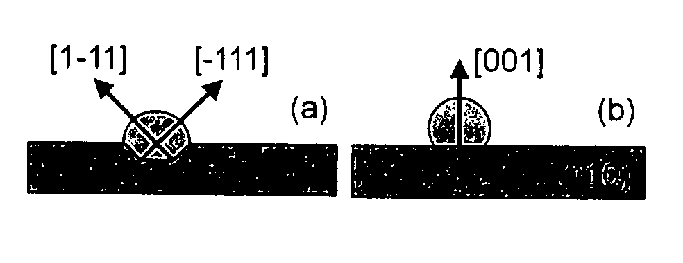
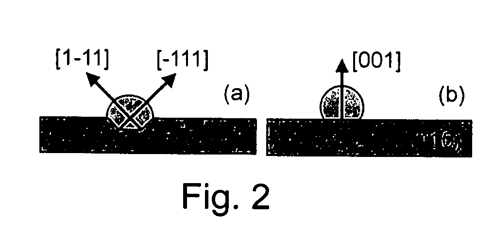
[0056] In accordance with the present invention, it is has been found that growth of a nanowhisker in a non-preferential direction (e.g., in an direction from an (001) crystal plane) is, once established, stable. The present invention more particularly recognizes the possibility to define and to stabilize the growth direction by controlling conditions at the onset of the nucleation event.

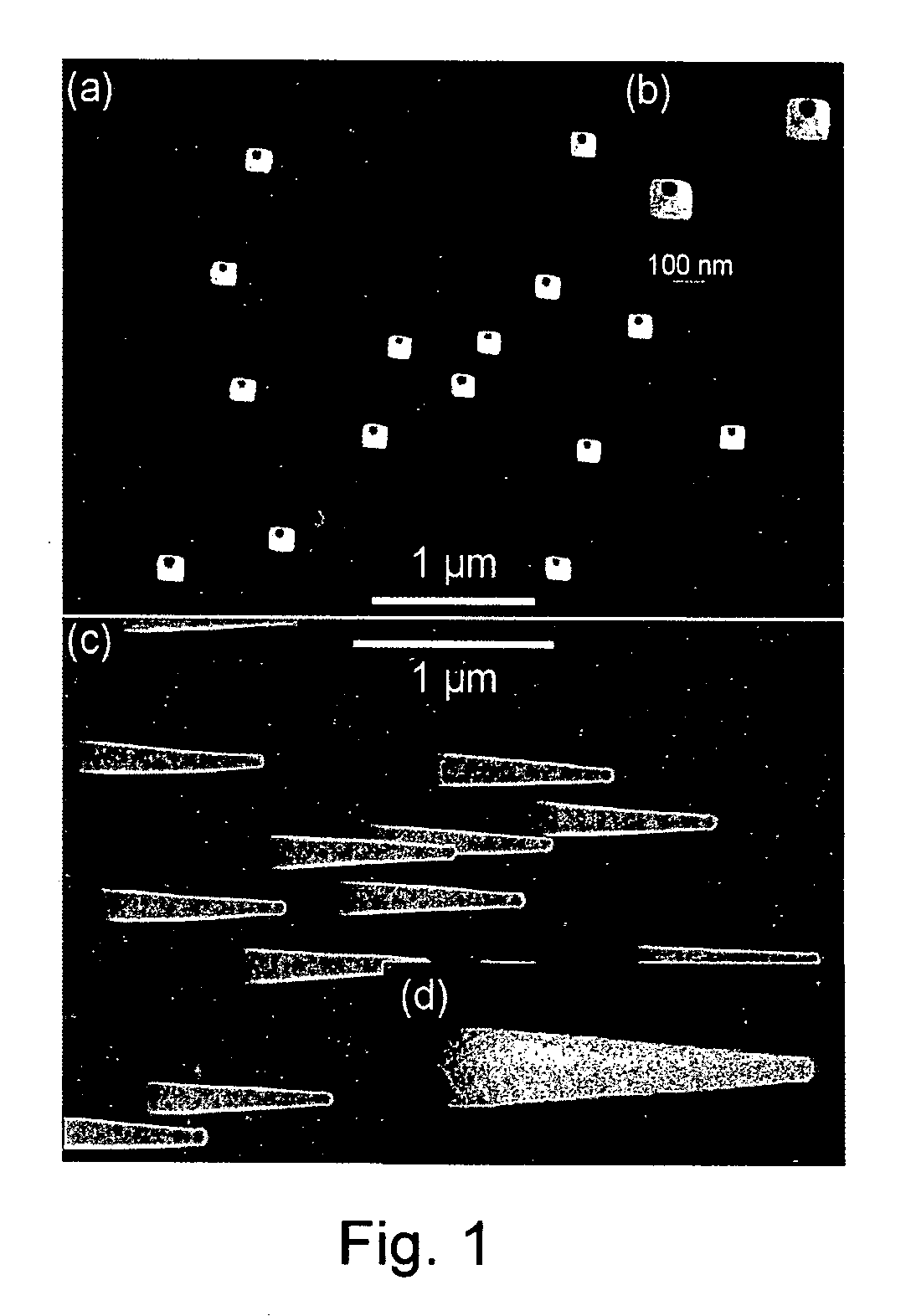
[0057] The following discussion describes an exemplary application of the invention to [001] InP nanowhiskers grown by metal-organic vapor phase epitaxy directly on (001) InP substrates. The nanowhiskers were characterized by scanning electron microscopy and transmission electron microscopy and found to have structural characteristics substantially superior to those of comparative whiskers grown in the preferential B direction, as will be discussed in detail below.

[0058] The InP nanowhiskers were grown using low-pressure metal-organic vapor phase epitaxy (MOVPE). Aerosol-produced, 50 nim Au-parti...


PUM

PropertyMeasurementUnit
Temperatureaaaaaaaaaa
Lengthaaaaaaaaaa
Structureaaaaaaaaaa

Abstract

Nanowhiskers are grown in a non-preferential growth direction by regulation of nucleation conditions to inhibit growth in a preferential direction. In a preferred implementation, <001> III-V semiconductor nanowhiskers are grown on an (001) III-V semiconductor substrate surface by effectively inhibiting growth in the preferential <111>B direction. As one example, <001> InP nano-wires were grown by metal-organic vapor phase epitaxy directly on (001) InP substrates. Characterization by scanning electron microscopy and transmission electron microscopy revealed wires with nearly square cross sections and a perfect zincblende crystalline structure that is free of stacking faults.

Description

CROSS-REFERENCE TO RELATED APPLICATIONS [0001] This application claims the benefit of the priority of U.S. Provisional Patent Application No. 60 / 541,949 filed Feb. 6, 2004, the entirety of which is incorporated herein by reference.BACKGROUND OF THE INVENTION [0002] 1. Field of the Invention [0003] This invention relates generally to structures produced by techniques of nanotechnology, and methods of producing such structures. More specifically, the invention relates to such structures and devices incorporating at least one element, essentially in one-dimensional form, which is of nanometer dimensions in its width or diameter, which is produced with the aid of a catalytic particle, and which is commonly termed a “nanowhisker.”[0004] 2. Background Art [0005] Nanotechnology covers various fields, including that of nanoengineering, which may be regarded as the practice of engineering on the nanoscale. This may result in structures ranging in size from small devices of atomic dimensions,...

Claims


Application Information

Patent Timeline
26 Jan 2006
Publication
US20060019470A1
IPC
H01L21/20; B01J23/52; C30B11/12; C30B25/00; C30B29/60; C30B29/62
CPC
B01J23/52; Y10S977/825; C30B11/12; C30B25/005; C30B29/605; C30B29/62; H01L21/02387; H01L21/02392
Inventors
SEIFERT, WERNER; SAMUELSON, LARS IVAR