Field effect transistor for chemical sensing using graphene, chemical sensor using the transistor and method for producing the transistor

a field effect transistor and chemical sensing technology, applied in the direction of material analysis, measurement devices, instruments by electric/magnetic means, etc., can solve the problems of not being realized as commercial products, risk of damage to the graphene layer, and not being able to achieve the effect of commercial products

Active Publication Date: 2015-10-13
GRAPHENSIC AB
View PDF8 Cites 1 Cited by
  • Summary
  • Abstract
  • Description
  • Claims
  • Application Information

AI Technical Summary

Benefits of technology

[0011]In view of the above, an object of this disclosure is to present a solution overcoming or at least alleviating problems in the prior art, or to at least present an alternative solution. A more specific object is to provide a field effect transistor for chemical sensing with graphene as the chemically sensitive material, thereby enabling low detection limits when the transistor is used as or in a chemical sensor, and, at the same time, enabling improvements in regard to robustness, reproducibility and / or individual variability. The invention is defined by the appended independent claims.
[0012]Hence, according to a first aspect there is provided a field effect transistor for chemical sensing, comprising a gate electrode, a drain electrode, a source electrode, and an electrically conducting and chemically sensitive channel extending between and being electrically connected to said drain electrode and source electrode, said gate electrode being arranged at a distance from and opposite to said chemically sensitive channel, so that the gate electrode and the chemically sensitive conducting channel are separated by a gap through which a chemical to be sensed can reach the chemically sensitive channel. The chemically sensitive channel comprises a continuous monocrystalline graphene layer arranged on an electrically insulating graphene layer substrate, the graphene layer extending between, and being electrically connected to, the source electrode and the drain electrode. The chemically sensitive channel and the grapheme layer substrate belong to a first separate part that is mounted to a second separate part comprising at least the gate electrode arranged on an insulating surface of a gate substrate. The substrate enables the graphene layer to be provided on a well defined surface and be produced and added to the transistor as a separate part. The substrate also supports the graphene layer and allows it to stay 2-dimensional, continuous and to remain in an intended position. This increases reproducibility and reduces the risk of damage to the graphene layer during production and after. In combination with the monocrystalline continuous graphene layer as such, this also enables low detection limits with low variability between individual transistors.
[0013]The graphene layer may have a uniform thickness, preferably a predetermined thickness of one or more monolayers of graphene. As the thickness effects electrical properties, e.g. band gap, carrier concentration etc., a uniform and preferably predetermined thickness provides control of the sensing properties and enables the formation of reproducible devices with low variability between individual sensors.
[0014]The graphene layer may be an epitaxial layer and the graphene layer substrate may be the substrate on which the graphene layer was epitaxially grown. By letting the graphene layer remain on the substrate of growth, it is not necessary to handle typically nano-thin graphene layers and structures. Also the risk of damaging the thin graphene layer during manufacturing of the transistor is reduced when the graphene layer can remain on the substrate.
[0022]In this way deposition or attachment of the drain electrode and the source electrode separately onto to the graphene layer of the chemically sensitive channel can be avoided. This is advantageous since it is known to be difficult to bond to graphene and processing, e.g. lithography, risks damage to the graphene layer (channel). Instead, when the parts are mounted separately, the electrodes can be pressed against, and in contact with, the chemically sensitive channel, for example by clamping the parts to each other. This also enables the size of the drain electrode and the source electrode to be used to control the height of the gap, which, when the parts are mounted to each other, may be determined by the thicknesses of the drain electrode and the source electrode, which preferably are equal in thickness, minus the thickness of the gate electrode.
[0031]Mounting as separate parts reduces the risk of damaging the graphene layer during manufacturing. Processing, e.g. lithography, which can be detrimental to the graphene layer can thereby be avoided in presence of the graphene layer. Instead processing of the second part can be made in isolation and the mounting of first part with the graphene layer can be performed in a later or last step during manufacturing.

Problems solved by technology

However, the sensor is not practical, accomplishing suspension by in situ-etching is cumbersome and is prone to result in differences in the suspension between individual sensors, risk of damage to the graphene layer during the etching and risk of damage to the graphene layer when the substrate has been etched away under it.
A general problem with this device, and often a general problem with many disclosed devices involving graphene at the present date or at present, is that they are mainly designed for experimental purposes and not to be realizable as commercial products for practical use.
They therefore, more often than not, have problems in areas such as robustness, reproducibility, individual variability, production yield and cost efficiency.
For example, when low detections limits are sought, it does not matter if one individual sensor can be made very sensitive if this is not repeatable so that many sensors with, in principle, equal sensitivity and low detection limit can be manufactured, or, if the sensor, during use or manufacture, is likely to or too easily may have its sensibility negatively affected.
Damage to the graphene layer may destroy or at least impair the chemical sensing capabilities.
Since the degree and impact of damages typically are, more or less, random in nature, also small damages may contribute to undesirable individual variability among sensors of the same type and construction, which may be a particular problem for sensors with low detection limits, as enabled by graphene.
However, the presented solution results in considerable differences in sensor response between individual devices with uncertainty of placement and thickness of the reduced graphene oxide platelets.
Also, the flexible nature of graphene makes suspension of an entire flake unlikely and thus contribution from the SiO2 substrate highly probable.

Method used


Image

  • Field effect transistor for chemical sensing using graphene, chemical sensor using the transistor and method for producing the transistor
  • Field effect transistor for chemical sensing using graphene, chemical sensor using the transistor and method for producing the transistor
  • Field effect transistor for chemical sensing using graphene, chemical sensor using the transistor and method for producing the transistor

Examples


Embodiment Construction

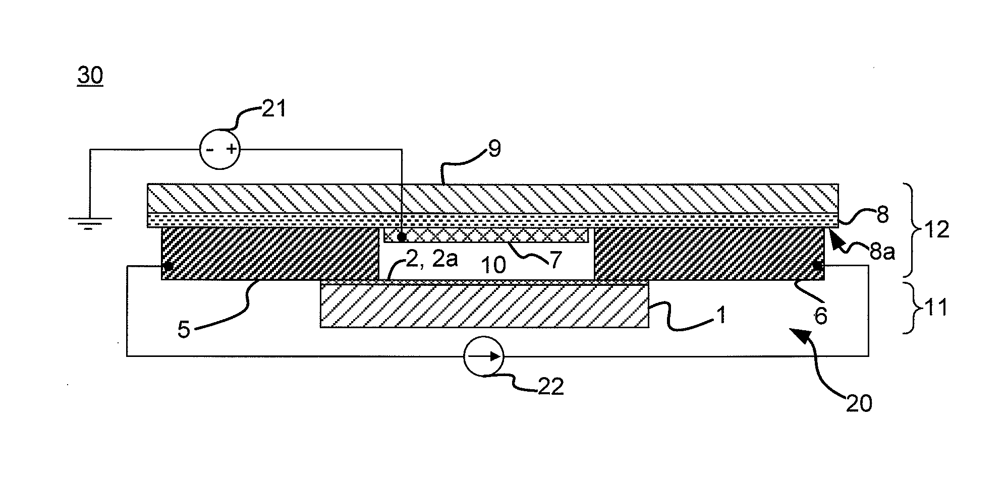
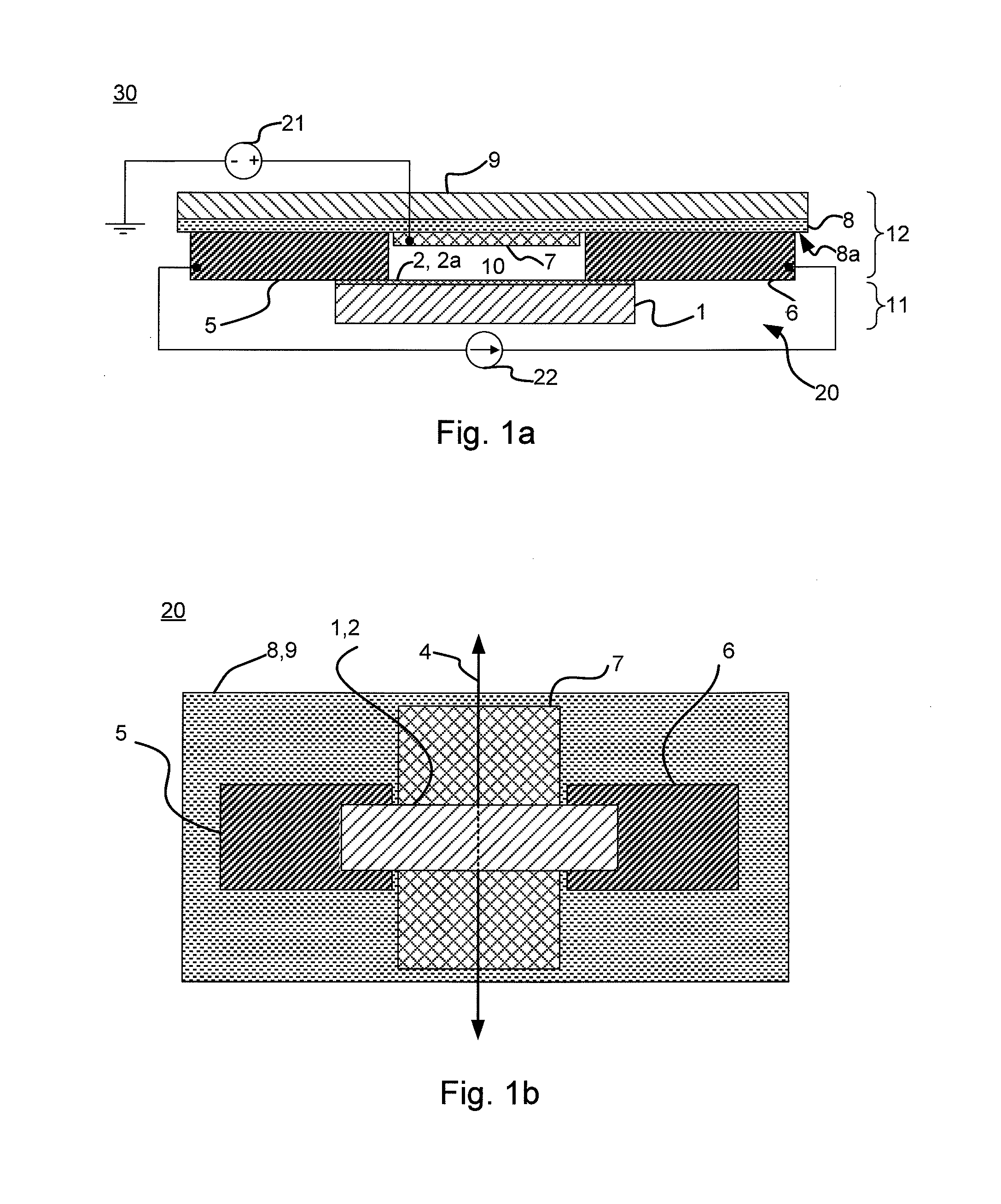
[0039]FIG. 1a schematically shows a side view of a field effect transistor 20 for chemical sensing according to a first embodiment and with schematic circuitry biasing the transistor for use as a chemical sensor 30. FIG. 1b schematically shows a bottom view of the field effect transistor 20 shown in FIG. 1a. Said figures display a design example of an air gap field effect gas sensor having a graphene layer supporting substrate 1, an electrically conducting and chemically sensitive channel 2, here formed by a continuous monocrystalline graphene layer 2a, a source electrode 5 in the form of a bonding pad, a drain electrode 6 in the form of a bonding pad, a gate electrode 7 in the form of a bonding pad, an electrically insulating gate substrate layer 8, a gate base substrate 9, and a gap 10. The chemically sensitive conducting channel 2 extends between and is electrically connected to the drain electrode 6 and the source electrode 5. The gate electrode 7 is arranged at a distance from ...


PUM

PropertyMeasurementUnit
widthaaaaaaaaaa
lengthaaaaaaaaaa
heightaaaaaaaaaa

Abstract

A field effect transistor (20) for chemical sensing, comprising an electrically conducting and chemically sensitive channel (2) extending between drain (5) and source (6) electrodes. A gate electrode (7) is separated from the channel (2) by a gap (10) through which a chemical to be sensed can reach the channel (2) which comprises a continuous monocrystalline graphene layer (2a) arranged on an electrically insulating graphene layer substrate (1). The graphene layer (2a) extends between and is electrically connected to the source electrode (5) and the drain electrode (6). The substrate supports the graphene layer, allowing it to stay 2-dimensional and continuous, and enables it to be provided on a well defined surface, and be produced and added to the transistor as a separate part. This is beneficial for reproducibility and reduces the risk of damage to the graphene layer during production and after. Low detection limits with low variability between individual transistors are also enabled. There is also provided a chemical sensor (30) using the transistor (20) and a method for providing the transistor (20).

Description

TECHNICAL FIELD[0001]The present disclosure relates generally to chemical sensing using field effect transistors and more particularly to chemical sensing using field effect transistors with a chemically sensitive channel involving graphene.TECHNICAL BACKGROUND[0002]Chemical sensing using field effect transistors (FETs), for example, a FET capable of detecting gas as described in the 1975 article I. Lundström, “A Hydrogen-Sensitive MOS Field-Effect Transistor” Applied Physics Letters 26, 55-57 and in U.S. Pat. No. 4,058,368 awarded to Svensson et. al. In the aforementioned article the transistor device has a palladium gate that is catalytically active with hydrogen dissociatively adsorbing and atomic hydrogen then absorbing into the palladium gate.[0003]Chemically sensitive FETs with an air gap between the channel and the gate have been described in e.g. Janata's 1985 U.S. Pat. Nos. 4,514,263 and 4,411,741 which describe a chemically sensitive field effect transistor with an air gap...

Claims


Application Information

Patent Timeline
Patent Type & Authority Patents(United States)
IPC IPC(8): H01L29/06G01N27/414
CPCG01N27/4146H01L29/0673G01N27/4141
Inventor ANDERSSON, MIKEHULTMAN, LARSLLOYD SPETZ, ANITAPEARCE, RUTHYAKIMOVA, ROSITSA
Owner GRAPHENSIC AB
Why Eureka
Try Eureka