

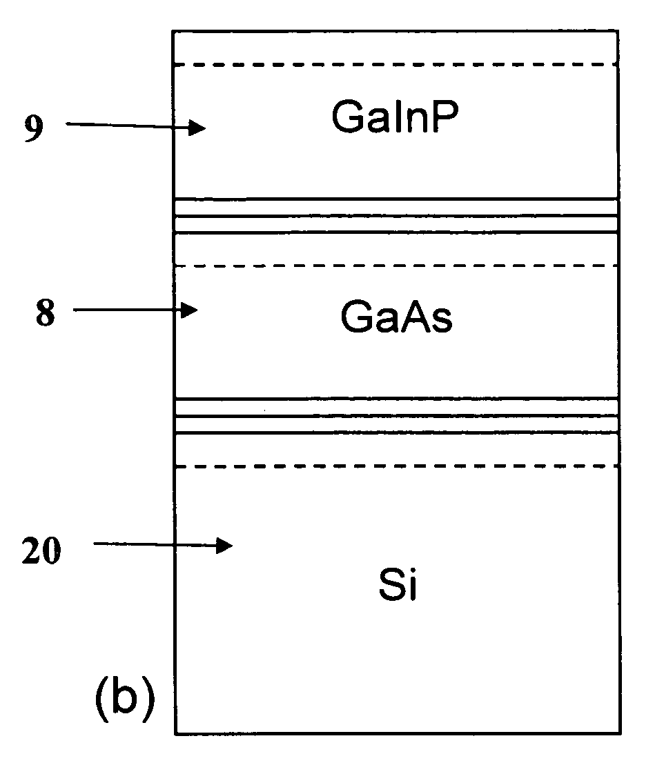
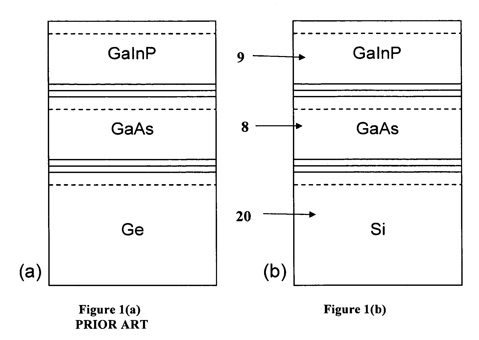
GaInP / GaAs / Si triple junction solar cell enabled by wafer bonding and layer transfer
a solar cell and wafer bonding technology, applied in the field of solar cells, can solve problems such as input materials
- Summary
- Abstract
- Description
- Claims
- Application Information
AI Technical Summary
Problems solved by technology
Method used
Image

Examples
first embodiment
Bonding and Layer Transfer of a Thin Ge Film to an Active-Si Substrate to Serve as a Heteroepitaxial Template
[0021] In the first embodiment, a process similar to the one described in U.S. patent application Ser. No. 10 / 251,33, filed on Dec. 19, 2002, entitled “Method of Using A Germanium Layer Transfer to Si For Photovoltaic Applications and Heterostructures Made Thereby”, incorporated herein by reference it its entirety, is applied to the bonding and layer transfer of a thin film or layer of Ge to the active-Si substrate. The integration scheme uses an extremely thin Ge film to minimize the band-to-band and free-carrier absorption of photons needed for the generation of photocurrent in the Si subcell. The use of heavily doped material achieves low specific resistance at the bonded interface and provides a large majority carrier density that can lead to reduced transmission.
[0022] A method for the integration of a GaInP / GaAs cell structure on active-Si in an “n-on-p” doping scheme ...
second embodiment
Bonding and Layer Transfer of a Thin GaAs Film to an Active-Si Substrate to Serve as a Heteroepitaxial Template Layer of the Second Embodiment
[0042] In the second embodiment, the thin, transferred, bonded Ge layer 5 is replaced with a thin, transferred, bonded GaAs layer 5. The rest of the process is similar to that of the first embodiment. The GaAs layer 5 may be exfoliated from a bulk, heavily doped GaAs wafer 5b or it may be exfoliated from a composite device substrate 5b comprising a GaAs film on a Ge substrate, as described in U.S. provisional patent application Ser. No. 60 / 564,251 filed Apr. 21, 2004 and a counterpart PCT application serial number PCT / US2005 / 013609 filed Apr. 21, 2005, both titled “A Method for the Fabrication of GaAs-Si Virtual Substrates” and both incorporated herein by reference in their entirety. In either case, the use of a thin GaAs layer or film (rather than Ge) as the epitaxial template mitigates the need to minimize the thickness of the transferred la...
fourth embodiment
Backside Strain or Bow Minimization Layer of the Fourth Embodiment
[0074] The fourth embodiment describes providing a backside film to control the bow or stress in the bonded substrates, such as Ge / Si or GaAs / Si substrates or other substrates described above. The film is formed on the back side of the silicon substrate of the silicon cell 20. However, the film may be used with other Ge / Si substrates that are not part of a GaInP / GaAs / Si triple junction solar cell. Any suitable back side film which compensates for the strain in the bonded substrate may be used, such as a metal silicide film. Other suitable films, such as insulating films with a coefficient of thermal expansion greater than that of silicon may be used. The film preferably has the following properties.
[0075] The film is compatible with MOCVD processing environments of at least 700° C. in reactive process gases, with no significant outgassing, no film relaxation and no contamination of the grown epitaxial film. The film ...
PUM
 Abstract
Description
Claims
Application Information