High-voltage MOS transistor and corresponding manufacturing method

Active Publication Date: 2006-02-02
ROBERT BOSCH GMBH
1 Cites 17 Cited by

AI-Extracted Technical Summary

Problems solved by technology

If the channel length is selected to be too small, then premature punch-through to the source occurs.
In particular, this causes the breakdown voltages to be unstable (walk out) and to drift as a function of loading (measuring conditions, wiring) and number of loadings.
The main disadvantage of this effect...

Benefits of technology

[0009] The high-voltage MOS transistor of the present invention, as well as the manufacturing method have the advantage that the avalanche breakdown is a volume breakdown and not a surface breakdown. The volume breakdown remains stable and produces an increased breakdown voltage, as well as an associated, expanded possible range of application. The temperature coefficient of the avalanche breakdown...

Abstract

A high-voltage MOS transistor having: a first region of a first conductivity type; a source region of the second conductivity type, which is introduced into the first region; a drain region of the second conductivity type, which is introduced into the first region; a channel region on the upper side of the first region, between the source region and the drain region; a field-oxide region in the drain region, between the source region and the drain region; a gate-oxide region over the channel region and between the edge of the drain region and the field-oxide region; a magnetoresistor region between the source region and the drain region, over the gate-oxide region and over at least a part of the field-oxide region; the drain region having a drain-terminal region and a drain-extension region and the doping profile of the drain-extension region is designed so that an avalanche breakdown occurs between the source region and the drain region, in a breakdown region that is on the edge of the drain-extension region and is not situated at the upper surface. Also it describes corresponding manufacturing methods.

Application Domain

TransistorThyristor +3

Technology Topic

Avalanche breakdownEngineering +5

Image

  • High-voltage MOS transistor and corresponding manufacturing method
  • High-voltage MOS transistor and corresponding manufacturing method
  • High-voltage MOS transistor and corresponding manufacturing method

Examples

  • Experimental program(3)

Example

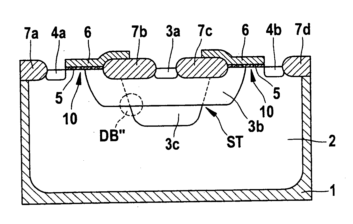
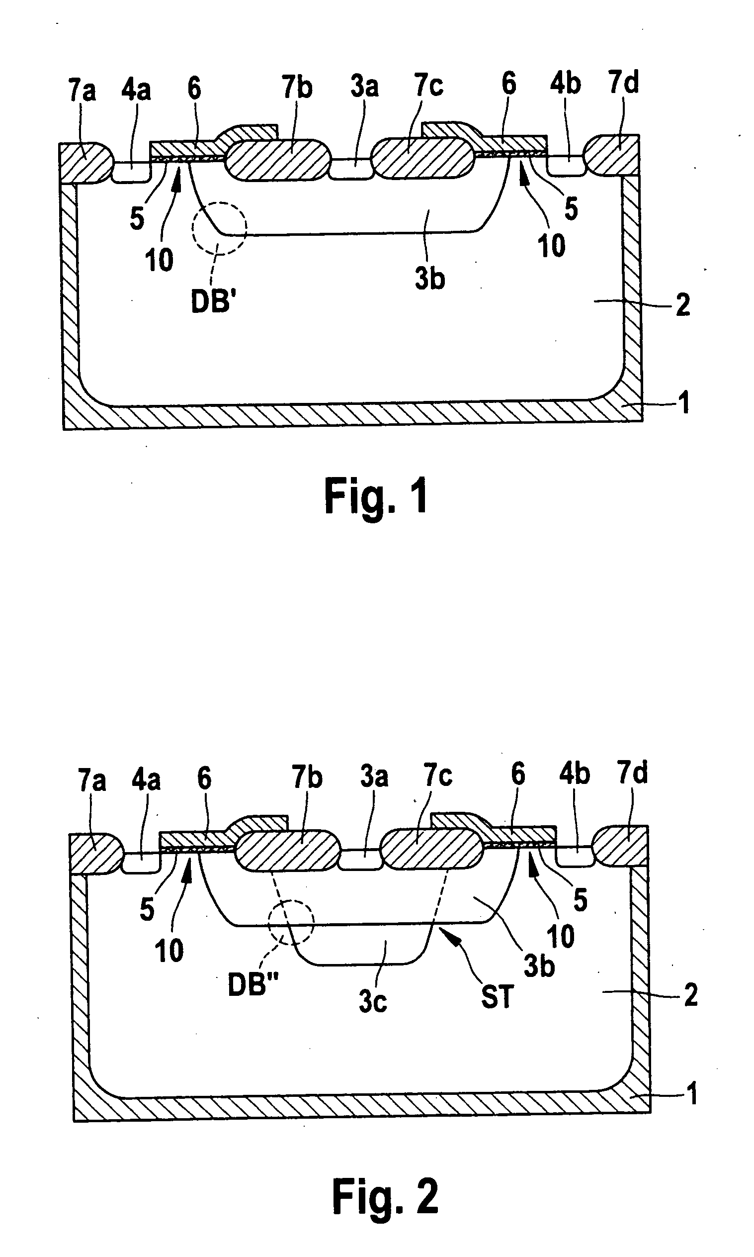
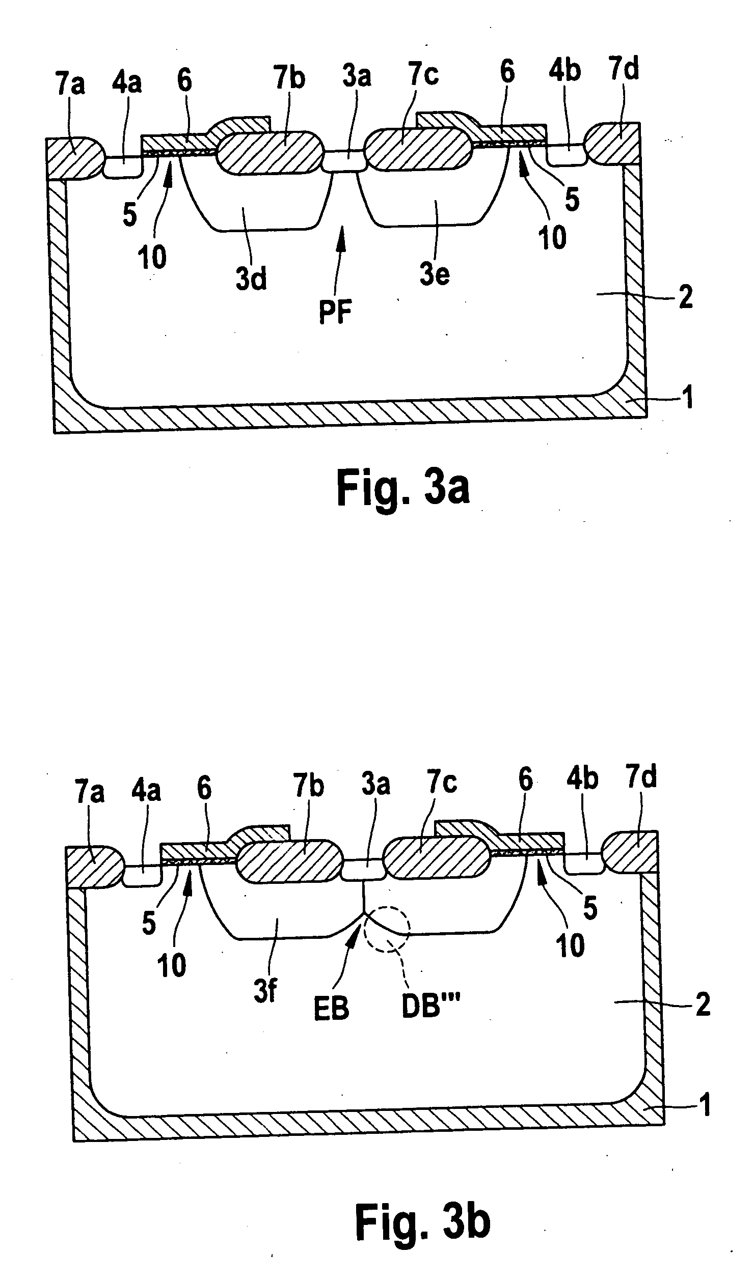
[0023]FIG. 1 shows a high-voltage MOS transistor according to a first specific embodiment of the present invention.
[0024] The high-voltage MOS transistor according to the first specific embodiment is a PMOS transistor integrated into a silicon p-semiconductor substrate 1, in which a first well 2 of the n-conductivity type is provided.
[0025] A strip-shaped drain region 3a, 3b of the p-conductivity type is introduced into first well 2, the drain region having a p+-drain terminal region 3a and a p-drain expansion region 3b. Two strip-shaped source regions 4a, 4b of the p+-conductivity type are introduced into first well 2 so as to be symmetric with respect to drain region 3a, 3b.
[0026] In each instance, a channel region 10 runs on the upper side of first well 2 between source region 4a or 4b and drain-extension region 3b. Field-oxide regions are designated by reference numerals 7a-d. Field-oxide regions 7b and 7c are situated on the upper side, in drain-extension region 3b, between drain-terminal region 3a and source regions 4a and 4b, respectively.
[0027] In each instance, a gate-oxide region 5 is situated above channel region 10 and on the upper side, between the edge of drain-extension region 3b and field-oxide region 7b or 7c. Magnetoresistor regions 6 extend between source region 4a or 4b and drain-terminal region 3a, over gate-oxide region 5 and over at least part of field-oxide regions 7b and 7c, respectively.
[0028] The doping profile (net doping, doping gradient) of drain-extension region 3b is designed so that an avalanche breakdown occurs between source region 4a or 4b and drain region 3a, 3b in a breakdown region DB′ at the edge of drain-extension region 3b, near its bottom side, breakdown region DB′ not being situated on the upper surface, i.e. a stable volume breakdown is present.
[0029] In practice, the doping profile may be ascertained by conventional simulations after determining the design of magnetoresistor regions 6. Generally speaking, desired breakdown region DB′ is reached and the avalanche-breakdown voltage is accordingly increased, as the net doping of p-drain expansion region 3b is less than, and gradient is flatter than, in the case of the related art, whereby interaction of the doping profile with magnetoresistor 6 must be taken into consideration. Such p-doping prevents premature penetration of the electric field through drain-extension region 3b to p+-drain terminal region 3a.

Example

[0030]FIG. 2 shows a high-voltage MOS transistor according to a second specific embodiment of the present invention.
[0031] In contrast to the first specific embodiment, the second specific embodiment shown in FIG. 2 provides an additional p-drain expansion region 3c, which has the shape of a well that is laterally smaller than the well shape of drain-extension region 3b and forms a step ST on the bottom side of the well of p-drain expansion region 3b. In this specific embodiment, the location of the avalanche breakdown, which is designated by DB″, is at step ST, i.e. further away from channel region 10 in the direction of the center of first p-drain expansion region 3b.
[0032]FIGS. 3a and b show a high-voltage MOS transistor in two production stages, according to a third specific embodiment of the present invention.

Example

[0033] In the third specific embodiment according to FIG. 3a, two discrete p-drain expansion regions 3c, 3d are produced by corresponding implantations, the two discrete p-drain expansion regions having a perforation region PF with respect to p+-drain terminal region 3a. In other words, p+-drain terminal region 3a opens out into n-well 2 in this perforation region PF. Starting out from this process state shown in FIG. 3a, a thermal diffusion treatment then occurs which causes discrete drain-extension regions 3c, 3d to fuse below p+-drain terminal region 3a.
[0034] In this specific embodiment, drain-extension region 3e resulting from it has an indentation EB below p+-drain terminal region 3a, the indentation causing the location of the avalanche breakdown DB′″ to be moved there, i.e. virtually below p+-drain terminal region 3a, and to consequently be even further away from channel region 10.
[0035]FIGS. 4a and b show a high-voltage MOS transistor in two production stages, according to a third specific embodiment of the present invention.
[0036] In contrast to the third specific embodiment, FIG. 4a provides for at least three discrete p-drain expansion regions 3g, 3h, 3i to be produced by corresponding implantations, the drain-extension regions having at least two perforation regions PF1, PF2.
[0037] Starting out from this process state shown in FIG. 4a, a thermal diffusion treatment then occurs which causes discrete drain-extension regions 3g, 3h, and 3i to fuse.
[0038] In this specific embodiment, drain-extension region 3j resulting from this has indentations EB1, EB2 below p+-drain terminal region 3a, the indentations causing the location of avalanche breakdown DB″″ to be moved there, i.e. virtually below p+-drain terminal region 3a, and to consequently be even further away from channel region 10.
[0039] Although the present invention was described above on the basis of preferred exemplary embodiments, it is not limited to them, but can be modified in various ways.
[0040] In particular, only symmetric, high-voltage PMOS transistors were described in the above-described specific embodiments, but the present invention is also applicable to high-voltage NMOS transistors and asymmetric, high-voltage PMOS transistors or high-voltage NMOS transistors.
LIST OF REFERENCE NUMERALS
[0041] 1,10 p-silicon semiconductor substrate [0042] 2,20 n-well [0043] 3a, 30a p-well, drain-terminal region [0044] 3b; 3b, 3c; [0045] 3f,3g,3h,3i,3j; [0046] 30b p-well; drain-extension region [0047] 3d,3e p-partial wells [0048] 4a,4b,40 n-source regions [0049] 5, 50 gate oxide [0050] 6, 60 magnetoresistor [0051] 7a-d, 70 field-oxide regions [0052] 10, 100 channel region [0053] DB,DB′, [0054] DB″,DB′″ [0055] DB″″ breakdown region [0056] ST step [0057] EB,EB1,EB2 indentation [0058] 80 n-well terminal [0059] PF,PF1,PF2 perforation region

PUM

no PUM

Description & Claims & Application Information

We can also present the details of the Description, Claims and Application information to help users get a comprehensive understanding of the technical details of the patent, such as background art, summary of invention, brief description of drawings, description of embodiments, and other original content. On the other hand, users can also determine the specific scope of protection of the technology through the list of claims; as well as understand the changes in the life cycle of the technology with the presentation of the patent timeline. Login to view more.

Similar technology patents

Package structure and forming method of the same

InactiveUS20200243430A1increase breakdown voltageincrease ability
Owner:DELTA ELECTRONICS INC

Method for producing electrostatic chuck and electrostatic chuck

ActiveUS20120248716A1suppress generation of particleincrease breakdown voltage
Owner:NGK INSULATORS LTD

Silicon carbide semiconductor device and method for manufacturing same

ActiveUS20150372128A1increase breakdown voltage
Owner:SUMITOMO ELECTRIC IND LTD

Multi-voltage level semiconductor device and its manufacture

InactiveUS7022574B2increase breakdown voltagereduce impurity
Owner:YAMAHA CORP

Classification and recommendation of technical efficacy words

  • increase breakdown voltage
  • expand range of application

Semiconductor device and method of manufacturing the same

InactiveUS6933565B2improve reliabilityincrease breakdown voltage
Owner:RENESAS ELECTRONICS CORP

Crystalline Semicondutor Film and Method for Manufacturing the Same

ActiveUS20090140255A1increase breakdown voltageimproved step coverage
Owner:SHARP KK

III-nitride device and method with variable epitaxial growth direction

ActiveUS20050191821A1increase breakdown voltageincrease current-carrying capacity
Owner:INFINEON TECH AMERICAS

Method for producing electrostatic chuck and electrostatic chuck

ActiveUS20120248716A1suppress generation of particleincrease breakdown voltage
Owner:NGK INSULATORS LTD

Hybrid surface-traversing apparatus and method

ActiveUS10919589B1expand range of applicationsignificant commercial value
Owner:INT CLIMBING MACHINES

Current Accumulative Pixel Structure for CMOS-TDI image sensor

InactiveUS20170180666A1reduce thermal noiseexpand range of application
Owner:TIANJIN UNIV

Direct liquid fuel cell power generation device

ActiveUS20200119377A1enhances low temperature environmental adaptabilityexpand range of application
Owner:DALIAN INST OF CHEM PHYSICS CHINESE ACAD OF SCI
Why Eureka
Try Eureka